SBVS100E June 2008 – September 2015 TPS720
PRODUCTION DATA.
- 1 Features
- 2 Applications
- 3 Description
- 4 Revision History
- 5 Pin Configuration and Functions
- 6 Specifications
- 7 Detailed Description
- 8 Application and Implementation
- 9 Power Supply Recommendations
- 10Layout
- 11Device and Documentation Support
- 12Mechanical, Packaging, and Orderable Information
Package Options
Mechanical Data (Package|Pins)
Thermal pad, mechanical data (Package|Pins)
- DRV|6
Orderable Information
3 Description
The TPS720 family of dual rail, low-dropout linear regulators (LDOs) offers outstanding ac performance (PSRR, load and line transient response), while consuming a very low quiescent current of 38 μA.
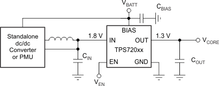
The VBIAS rail that powers the control circuit of the LDO draws very low current (on the order of the quiescent current of the LDO) and can be connected to any power supply that is equal to or greater than 1.4 V above the output voltage. The main power path is through VIN, which can be a lower voltage than VBIAS; it can be as low as VOUT + VDO, increasing the efficiency of the solution in many power-sensitive applications. For example, VIN can be an output of a high-efficiency, DC-DC step-down regulator.
The TPS720 supports a novel feature in which the output of the LDO regulates under light loads when the IN pin is left floating. The light-load drive current is sourced from VBIAS under this condition. This feature is particularly useful in power-saving applications where the DC-DC converter connected to the IN pin is disabled but the LDO is still required to regulate the voltage to a light load.
The TPS720 is stable with ceramic capacitors and uses an advanced BICMOS fabrication process that yields a dropout of 110 mV at a 350-mA output load. The TPS720 has the unique feature of providing a monotonic VOUT rise (overshoot limited to 3%) with VIN inrush current limited to 100 mA + ILOAD with an output capacitor of 2.2 μF.
The TPS720 uses a precision voltage reference and feedback loop to achieve overall accuracy of 2% over load, line, process, and temperature extremes. An ultra-small DSBGA package makes the TPS720 ideal for handheld applications. The TPS720 is also available in a SON-8 package. This family of devices is fully specified over the temperature range of
TJ = –40°C to 125°C.
Device Information(1)
| PART NUMBER | PACKAGE | BODY SIZE (NOM) |
|---|---|---|
| TPS720 | DSBGA (5) | 1.36 mm × 0.96 mm |
| SON (6) | 2.00 mm × 2.00 mm |
- For all available packages, see the orderable addendum at the end of the data sheet.
Simplified Schematic
