SBVS100E June   2008  – September 2015 TPS720

PRODUCTION DATA.  

  1. Features
  2. Applications
  3. Description
    1.     Simplified Schematic
  4. Revision History
  5. Pin Configuration and Functions
    1.     Pin Functions
  6. Specifications
    1. 6.1 Absolute Maximum Ratings
    2. 6.2 ESD Ratings
    3. 6.3 Recommended Operating Conditions
    4. 6.4 Thermal Information
    5. 6.5 Electrical Characteristics
    6. 6.6 Typical Characteristics
  7. Detailed Description
    1. 7.1 Overview
    2. 7.2 Functional Block Diagram
    3. 7.3 Feature Description
      1. 7.3.1 Internal Current Limit
      2. 7.3.2 Inrush Current Limit
      3. 7.3.3 Shutdown
      4. 7.3.4 Undervoltage Lockout (UVLO)
    4. 7.4 Device Functional Modes
  8. Application and Implementation
    1. 8.1 Application Information
      1. 8.1.1 Input and Output Capacitor Requirements
      2. 8.1.2 Output Regulation With IN Pin Floating
      3. 8.1.3 Dropout Voltage
      4. 8.1.4 Transient Response
      5. 8.1.5 Minimum Load
    2. 8.2 Typical Application
      1. 8.2.1 Design Requirements
      2. 8.2.2 Detailed Design Procedures
      3. 8.2.3 Application Curves
  9. Power Supply Recommendations
  10. 10Layout
    1. 10.1 Layout Guidelines
    2. 10.2 Layout Example
    3. 10.3 Thermal Considerations
    4. 10.4 Power Dissipation
  11. 11Device and Documentation Support
    1. 11.1 Device Support
      1. 11.1.1 Development Support
        1. 11.1.1.1 Evaluation Module
      2. 11.1.2 Device Nomenclature
    2. 11.2 Documentation Support
      1. 11.2.1 Related Documentation
    3. 11.3 Community Resources
    4. 11.4 Trademarks
    5. 11.5 Electrostatic Discharge Caution
    6. 11.6 Glossary
  12. 12Mechanical, Packaging, and Orderable Information
    1. 12.1 Package Mounting

Package Options

Mechanical Data (Package|Pins)
Thermal pad, mechanical data (Package|Pins)
Orderable Information

Typical Characteristics

Over operating temperature range (TJ = –40°C to 125°C), VBIAS = (VOUT + 1.4 V) or 2.5 V (whichever is greater); VIN = VOUT + 0.5 V, IOUT = 1 mA, VEN = 1.1 V, COUT = 2.2 μF, unless otherwise noted. Typical values are at TJ = 25°C.
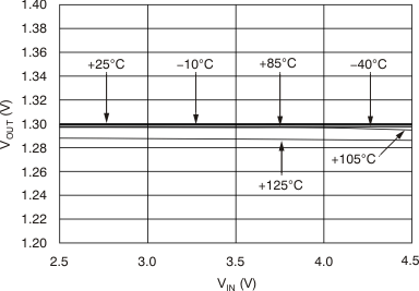
TPS720 tc_line_vin_0_bvs100.gif
IOUT = 0 mA
Figure 1. VIN Line Regulation (TPS72013YZU)
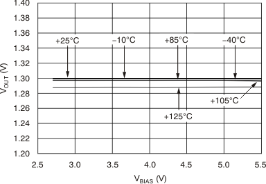
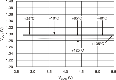
TPS720 tc_line_vbias_0_bvs100.gif
IOUT = 0 mA
Figure 3. VBIAS Line Regulation (TPS72013YZU)
TPS720 tc_load_light_bvs100.gif
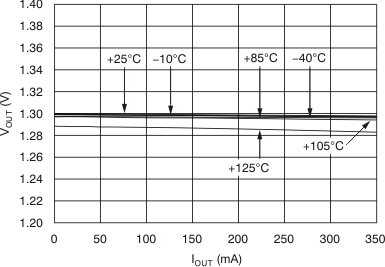
Figure 5. Load Regulation Under Light Loads (TPS72013YZU)
TPS720 tc_load_vbias_bvs100.gif
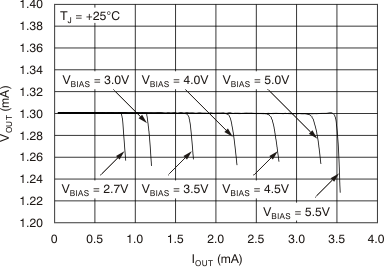
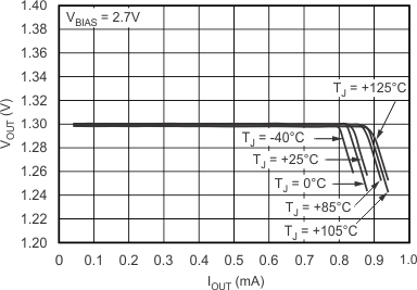
Figure 7. Load Regulation With VIN Floating (TPS72013YZU)
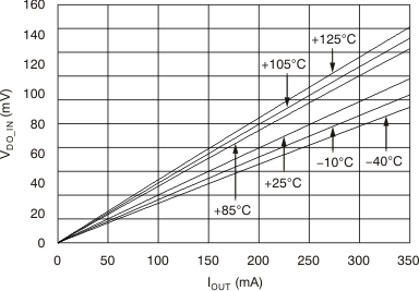
TPS720 tc_vdo-iout_bvs100.gif
Figure 9. VIN Dropout Voltage vs Output Current (TPS72013YZU)
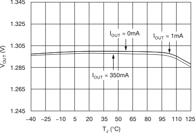
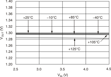
TPS720 tc_vout-tmp_bvs100.gif
Figure 11. Output Voltage vs Temperature (TPS72013YZU)
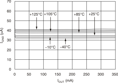
TPS720 tc_ignd-iout_bvs100.gif
Figure 13. Ground Pin Current vs Output Current (TPS72013YZU)
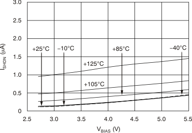
TPS720 tc_ishdn-vbias_bvs100.gif
Figure 15. Shutdown Current vs VBIAS Input Voltage (TPS72013YZU)
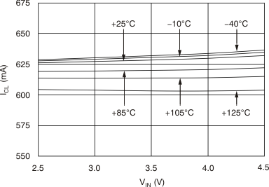
TPS720 tc_icl-vin_bvs100.gif
Figure 17. Current Limit vs VIN Input Voltage (TPS72013YZU)
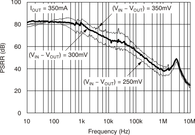
TPS720 tc_psrr-frq_iout_bvs100.gif
Figure 19. VIN Power-Supply Ripple Rejection
vs Frequency (TPS72015YZU)
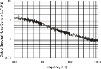
TPS720 tc_noise-frq_bvs100.gif
Figure 21. Output Spectral Noise Density vs Frequency (TPS72015YZU)
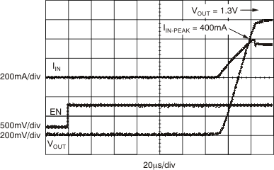
TPS720 tc_inrush_350ma_bvs100.gif
VIN = 1.8 V VOUT = 1.3 V VBIAS = 2.7 V
IOUT = 350 mA
Figure 23. VIN Inrush Current
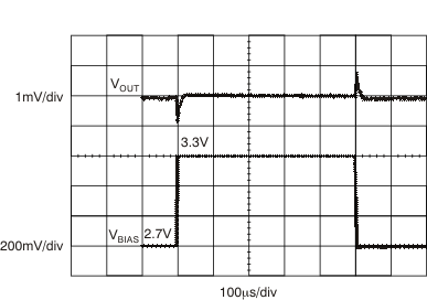
TPS720 tc_line_resp_vbias_bvs100.gif
VIN = 1.8 V VOUT = 1.3 V VBIAS = 2.7 V to 3.3 V
VBIAS Slew Rate = 600 m/μs IOUT = 350 mA
Figure 25. VBIAS Line Transient Response
TPS720 tc_line_vin_350_bvs100.gif
IOUT = 350 mA
Figure 2. VIN Line Regulation (TPS72013YZU)
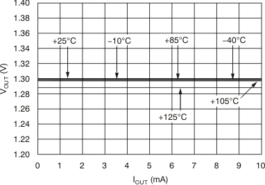
TPS720 tc_line_vbias_350_bvs100.gif
IOUT = 350 mA
Figure 4. VBIAS Line Regulation (TPS72013YZU)
TPS720 tc_load_reg_bvs100.gif
Figure 6. Load Regulation (TPS72013YZU)
TPS720 tc_load_tj_bvs100.gif
Figure 8. Load Regulation With VIN Floating (TPS72013YZU)
TPS720 tc_vdo-tmp_bvs100.gif
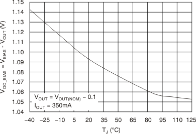
Figure 10. VBIAS Dropout Voltage vs Temperature (TPS72033YZU)
TPS720 tc_ignd-vbias_bvs100.gif
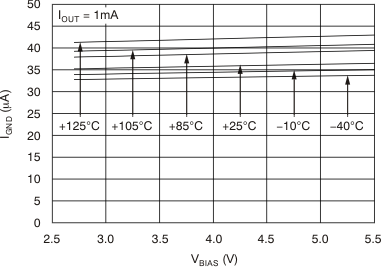
Figure 12. Ground Pin Current vs VBIAS Input Voltage (TPS72013YZU)
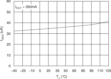
TPS720 tc_ignd-tmp_bvs100.gif
Figure 14. Ground Pin Current vs Temperature (TPS72013YZU)
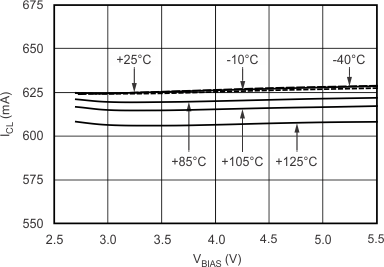
TPS720 tc_icl-vbias_bvs100.gif
Figure 16. Current Limit vs VBIAS Input Voltage (TPS72013YZU)
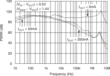
TPS720 tc_psrr-frq_vin_bvs100.gif
Figure 18. VIN Power-Supply Ripple Rejection vs Frequency (TPS72015YZU)
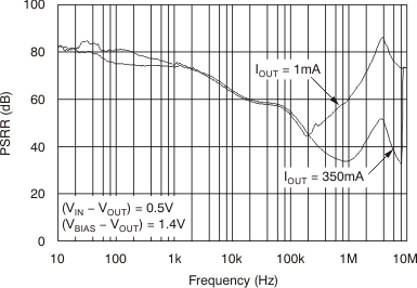
TPS720 tc_psrr-frq_vbias_bvs100.gif
Figure 20. VBIAS Power-Supply Ripple Rejection vs Frequency (TPS72015YZU)
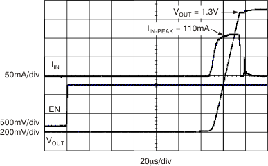
TPS720 tc_inrush_0ma_bvs100.gif
VIN = 1.8 V VOUT = 1.3 V VBIAS = 2.7 V
IOUT = 0 mA
Figure 22. VIN Inrush Current
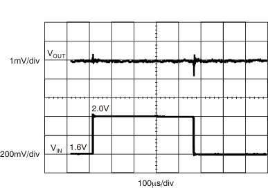
TPS720 tc_line_resp_vin_bvs100.gif
VIN = 1.6 to 2 V VOUT = 1.3 V VBIAS = 2.7 V
VIN Slew Rate = 1 V/μs IOUT = 350 mA
Figure 24. VIN Line Transient Response
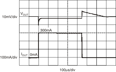
TPS720 tc_load_resp_bvs100.gif
VIN = 1.8 V VOUT = 1.3 V VBIAS = 2.7 V
tRISE = 1 μs
Figure 26. Load Transient Response