SBVS100E June 2008 – September 2015 TPS720
PRODUCTION DATA.
- 1 Features
- 2 Applications
- 3 Description
- 4 Revision History
- 5 Pin Configuration and Functions
- 6 Specifications
- 7 Detailed Description
- 8 Application and Implementation
- 9 Power Supply Recommendations
- 10Layout
- 11Device and Documentation Support
- 12Mechanical, Packaging, and Orderable Information
Package Options
Mechanical Data (Package|Pins)
Thermal pad, mechanical data (Package|Pins)
- DRV|6
Orderable Information
5 Pin Configuration and Functions
DRV Package
6-Pin SON With Exposed Thermal Pad
Top View

1. TI recommends connecting the SON (DRV) package thermal pad to ground.
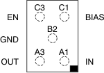
YZU Package
5-Pin DSBGA
Top View

Pin Functions
| PIN | I/O | DESCRIPTION | ||
|---|---|---|---|---|
| NAME | DRV | YZU | ||
| OUT | 1 | A3 | O | Output pin. A 2.2-μF ceramic capacitor is connected from this pin to ground, for stability and to provide load transients. See Input and Output Capacitor Requirements. |
| NC | 2 | — | — | No connection. |
| EN | 3 | C3 | I | Enable pin. A logic high signal on this pin turns the device on and regulates the voltage from IN to OUT. A logic low on this pin turns off the device. |
| BIAS | 4 | C1 | I | Bias supply pin. TI recommends bypassing this input with a ceramic capacitor to ground for better transient performance. See Input and Output Capacitor Requirements. |
| GND | 5 | B2 | — | Ground pin. |
| IN | 6 | A1 | I | Input pin. This pin can be a maximum of 4.5 V; VIN must not exceed VBIAS. Bypass this input with a ceramic capacitor to ground. See Input and Output Capacitor Requirements. |