SLVS351Q September   2002  – June 2025 TPS796

PRODUCTION DATA  

  1.   1
  2. Features
  3. Applications
  4. Description
  5. Pin Configuration and Functions
  6. Specifications
    1. 5.1 Absolute Maximum Ratings
    2. 5.2 ESD Ratings
    3. 5.3 Recommended Operating Conditions
    4. 5.4 Thermal Information
    5. 5.5 Electrical Characteristics
    6. 5.6 Typical Characteristics
  7. Detailed Description
    1. 6.1 Overview
    2. 6.2 Functional Block Diagrams
    3. 6.3 Feature Description
      1. 6.3.1 Active Discharge (New Chip)
      2. 6.3.2 Shutdown
      3. 6.3.3 Start-Up
      4. 6.3.4 Undervoltage Lockout (UVLO)
      5. 6.3.5 Regulator Protection
        1. 6.3.5.1 Current Limit
        2. 6.3.5.2 Thermal Shutdown
    4. 6.4 Device Functional Modes
      1. 6.4.1 Normal Operation
      2. 6.4.2 Dropout Operation
      3. 6.4.3 Disabled
  8. Application and Implementation
    1. 7.1 Application Information
      1. 7.1.1 Recommended Capacitor Types
      2. 7.1.2 Input and Output Capacitor Requirements
      3. 7.1.3 Feed-forward Capacitor (CFF)
      4. 7.1.4 Adjustable Configuration
      5. 7.1.5 Load Transient Response
      6. 7.1.6 Dropout Voltage
        1. 7.1.6.1 Exiting Dropout
      7. 7.1.7 Noise Reduction Pin (legacy chip)
      8. 7.1.8 Power Dissipation (PD)
    2. 7.2 Typical Application
      1. 7.2.1 Design Requirements
      2. 7.2.2 Detailed Design Procedure
      3. 7.2.3 Application Curves
      4. 7.2.4 Best Design Practices
    3. 7.3 Power Supply Recommendations
    4. 7.4 Layout
      1. 7.4.1 Layout Guidelines
        1. 7.4.1.1 Board Layout Recommendation to Improve PSRR and Noise Performance
        2. 7.4.1.2 Regulator Mounting
        3. 7.4.1.3 Estimating Junction Temperature
      2. 7.4.2 Layout Examples
  9. Device and Documentation Support
    1. 8.1 Device Support
      1. 8.1.1 Development Support
        1. 8.1.1.1 Evaluation Modules
        2. 8.1.1.2 Spice Models
      2. 8.1.2 Device Nomenclature
    2. 8.2 Documentation Support
      1. 8.2.1 Related Documentation
    3. 8.3 Receiving Notification of Documentation Updates
    4. 8.4 Support Resources
    5. 8.5 Trademarks
    6. 8.6 Electrostatic Discharge Caution
    7. 8.7 Glossary
  10. Revision History
  11. 10Mechanical, Packaging, and Orderable Information

Package Options

Mechanical Data (Package|Pins)
Thermal pad, mechanical data (Package|Pins)
Orderable Information

Typical Characteristics

at VEN = VIN, VIN = VOUT(nom) + 1V, IOUT = 1mA, COUT = 10µF, CNR = 0.01µF, CIN = 2.2µF, and TJ = 25°C (unless otherwise noted)

TPS796 TPS79630 Output Voltage vs
                        Output Current
Legacy chip
Figure 5-1 TPS79630 Output Voltage vs Output Current
TPS796 TPS79628 Output Voltage vs
                        Junction Temperature
Legacy chip
Figure 5-3 TPS79628 Output Voltage vs Junction Temperature
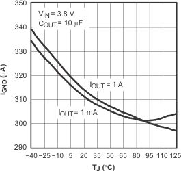
TPS796 TPS79628 Ground Current vs
                        Junction Temperature
Legacy chip
Figure 5-5 TPS79628 Ground Current vs Junction Temperature
TPS796 TPS79630 Output Spectral
                        Noise Density vs Frequency
Legacy chip
Figure 5-7 TPS79630 Output Spectral Noise Density vs Frequency
TPS796 TPS79630 Output Spectral
                        Noise Density vs Frequency
Legacy chip
Figure 5-9 TPS79630 Output Spectral Noise Density vs Frequency
TPS796 TPS79633 Output Spectral
                        Noise Density vs Frequency
COUT = 10uF (new chip)
Figure 5-11 TPS79633 Output Spectral Noise Density vs Frequency
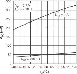
TPS796 TPS79628 Dropout Voltage
                        vs Junction Temperature
Legacy chip
Figure 5-13 TPS79628 Dropout Voltage vs Junction Temperature
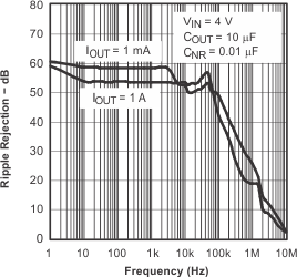
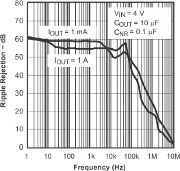
TPS796 TPS79630 Ripple Rejection
                        vs Frequency
Legacy chip
Figure 5-15 TPS79630 Ripple Rejection vs Frequency
TPS796 TPS79630 Ripple Rejection
                        vs Frequency
Legacy chip
Figure 5-17 TPS79630 Ripple Rejection vs Frequency
TPS796 TPS79633 Ripple Rejection
                        vs Frequency
COUT = 1uF (new chip)
Figure 5-19 TPS79633 Ripple Rejection vs Frequency
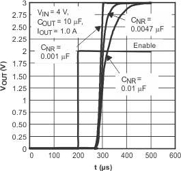
TPS796 Start-Up Time
New chip
Figure 5-21 Start-Up Time
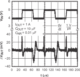
TPS796 TPS79630 Line Transient
                        Response
Legacy chip
Figure 5-23 TPS79630 Line Transient Response
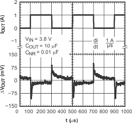
TPS796 TPS79628 Load Transient
                        Response
Legacy chip
Figure 5-25 TPS79628 Load Transient Response
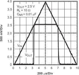
TPS796 TPS79625 Power-Up,
                        Power-Down
Legacy chip
Figure 5-27 TPS79625 Power-Up, Power-Down
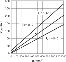
TPS796 TPS79630 Dropout Voltage
                        vs Output Current
Legacy chip
Figure 5-29 TPS79630 Dropout Voltage vs Output Current
TPS796 TPS79630 Typical Regions
                        of Stability Equivalent Series Resistance (ESR) vs Output Current
Legacy chip
Figure 5-31 TPS79630 Typical Regions of Stability Equivalent Series Resistance (ESR) vs Output Current
TPS796 TPS79630 Typical Regions
                        of Stability Equivalent Series Resistance (ESR) vs Output Current
Legacy chip
Figure 5-33 TPS79630 Typical Regions of Stability Equivalent Series Resistance (ESR) vs Output Current
TPS796 TPS79633 Output Voltage vs
                        Output Current
New chip
Figure 5-2 TPS79633 Output Voltage vs Output Current
TPS796 TPS79633 Output Voltage vs
                        Junction Temperature
New chip
Figure 5-4 TPS79633 Output Voltage vs Junction Temperature
TPS796 TPS79633 Ground Current vs
                        Junction Temperature
New chip
Figure 5-6 TPS79633 Ground Current vs Junction Temperature
TPS796 TPS79633 Output Spectral
                        Noise Density vs Frequency
COUT = 2.2uF (new chip)
Figure 5-8 TPS79633 Output Spectral Noise Density vs Frequency
TPS796 TPS79630 Output Spectral
                        Noise Density vs Frequency
Legacy chip
Figure 5-10 TPS79630 Output Spectral Noise Density vs Frequency
TPS796 TPS79630 Root Mean Squared
                        Output Noise vs Bypass Capacitance
Legacy chip
Figure 5-12 TPS79630 Root Mean Squared Output Noise vs Bypass Capacitance
TPS796 TPS79633 Dropout Voltage
                        vs Junction Temperature
New chip
Figure 5-14 TPS79633 Dropout Voltage vs Junction Temperature
TPS796 TPS79630 Ripple Rejection
                        vs Frequency
Legacy chip
Figure 5-16 TPS79630 Ripple Rejection vs Frequency
TPS796 TPS79633 Ripple Rejection
                        vs Frequency
New chip
Figure 5-18 TPS79633 Ripple Rejection vs Frequency
TPS796 Start-Up Time
Legacy chip
Figure 5-20 Start-Up Time
TPS796 TPS79618 Line Transient
                        Response
Legacy chip
Figure 5-22 TPS79618 Line Transient Response
TPS796 TPS79633 Line Transient
                        Response
New chip
Figure 5-24 TPS79633 Line Transient Response
TPS796 TPS79633 Load Transient
                        Response
New chip
Figure 5-26 TPS79633 Load Transient Response
TPS796 TPS79633 Power-Up,
                        Power-Down
New chip
Figure 5-28 TPS79633 Power-Up, Power-Down
TPS796 TPS79633 Dropout Voltage
                        vs Output Current
New chip
Figure 5-30 TPS79633 Dropout Voltage vs Output Current
TPS796 TPS79630 Typical Regions
                        of Stability Equivalent Series Resistance (ESR) vs Output Current
Legacy chip
Figure 5-32 TPS79630 Typical Regions of Stability Equivalent Series Resistance (ESR) vs Output Current