SLVS351Q September   2002  – June 2025 TPS796

PRODUCTION DATA  

  1.   1
  2. Features
  3. Applications
  4. Description
  5. Pin Configuration and Functions
  6. Specifications
    1. 5.1 Absolute Maximum Ratings
    2. 5.2 ESD Ratings
    3. 5.3 Recommended Operating Conditions
    4. 5.4 Thermal Information
    5. 5.5 Electrical Characteristics
    6. 5.6 Typical Characteristics
  7. Detailed Description
    1. 6.1 Overview
    2. 6.2 Functional Block Diagrams
    3. 6.3 Feature Description
      1. 6.3.1 Active Discharge (New Chip)
      2. 6.3.2 Shutdown
      3. 6.3.3 Start-Up
      4. 6.3.4 Undervoltage Lockout (UVLO)
      5. 6.3.5 Regulator Protection
        1. 6.3.5.1 Current Limit
        2. 6.3.5.2 Thermal Shutdown
    4. 6.4 Device Functional Modes
      1. 6.4.1 Normal Operation
      2. 6.4.2 Dropout Operation
      3. 6.4.3 Disabled
  8. Application and Implementation
    1. 7.1 Application Information
      1. 7.1.1 Recommended Capacitor Types
      2. 7.1.2 Input and Output Capacitor Requirements
      3. 7.1.3 Feed-forward Capacitor (CFF)
      4. 7.1.4 Adjustable Configuration
      5. 7.1.5 Load Transient Response
      6. 7.1.6 Dropout Voltage
        1. 7.1.6.1 Exiting Dropout
      7. 7.1.7 Noise Reduction Pin (legacy chip)
      8. 7.1.8 Power Dissipation (PD)
    2. 7.2 Typical Application
      1. 7.2.1 Design Requirements
      2. 7.2.2 Detailed Design Procedure
      3. 7.2.3 Application Curves
      4. 7.2.4 Best Design Practices
    3. 7.3 Power Supply Recommendations
    4. 7.4 Layout
      1. 7.4.1 Layout Guidelines
        1. 7.4.1.1 Board Layout Recommendation to Improve PSRR and Noise Performance
        2. 7.4.1.2 Regulator Mounting
        3. 7.4.1.3 Estimating Junction Temperature
      2. 7.4.2 Layout Examples
  9. Device and Documentation Support
    1. 8.1 Device Support
      1. 8.1.1 Development Support
        1. 8.1.1.1 Evaluation Modules
        2. 8.1.1.2 Spice Models
      2. 8.1.2 Device Nomenclature
    2. 8.2 Documentation Support
      1. 8.2.1 Related Documentation
    3. 8.3 Receiving Notification of Documentation Updates
    4. 8.4 Support Resources
    5. 8.5 Trademarks
    6. 8.6 Electrostatic Discharge Caution
    7. 8.7 Glossary
  10. Revision History
  11. 10Mechanical, Packaging, and Orderable Information

Package Options

Mechanical Data (Package|Pins)
Thermal pad, mechanical data (Package|Pins)
Orderable Information

Pin Configuration and Functions

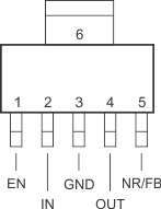
TPS796 DCQ Package, 6-Pin SOT-223
                            (Top View, Legacy Chip)Figure 4-1 DCQ Package, 6-Pin SOT-223
(Top View, Legacy Chip)
TPS796 KTT Package, 5-Pin TO-263
                            (Top View, Legacy Chip)Figure 4-3 KTT Package, 5-Pin TO-263
(Top View, Legacy Chip)
Figure 4-2 DCQ Package, 6-Pin SOT-223
(Top View, New Chip)
TPS796 DRB Package, 8-Pin VSON
                            (Top View, Legacy Chip)Figure 4-4 DRB Package, 8-Pin VSON
(Top View, Legacy Chip)
Figure 4-5 DRB Package, 8-Pin VSON
(Top View, New Chip)
Table 4-1 Pin Functions
PIN TYPE DESCRIPTION
NAME SOT-223
TO-263
VSON
EN 1 8 I Enable pin. Driving the enable pin (EN) high turns on the regulator. Driving this pin low puts the regulator into shutdown mode. EN can be connected to IN if not used.
FB 5 5 I Feedback pin. This terminal is the feedback input voltage for the adjustable device.
GND 3, Tab 6, PowerPAD Regulator ground
IN 2 1, 2 I Input to the device.
N/C 5 7 Not internally connected. This pin must either be left open, or tied to GND.
NR 5 5 Noise-reduction pin (legacy chip). Connecting an external capacitor to this pin bypasses noise generated by the internal band gap. This bypass improves power-supply rejection and reduces output noise. For a lower noise performance device, consider the TPS7A91.
OUT 4 3, 4 O Output of the regulator.