SLVS351Q September 2002 – June 2025 TPS796
PRODUCTION DATA
- 1
- 1 Features
- 2 Applications
- 3 Description
- 4 Pin Configuration and Functions
- 5 Specifications
- 6 Detailed Description
- 7 Application and Implementation
- 8 Device and Documentation Support
- 9 Revision History
- 10Mechanical, Packaging, and Orderable Information
Package Options
Mechanical Data (Package|Pins)
Thermal pad, mechanical data (Package|Pins)
Orderable Information
7.1.4 Adjustable Configuration
The output voltage of the TPS79601 adjustable regulator is programmed using an external resistor divider, as Figure 7-1 shows.
 Figure 7-1 Typical
Application, Adjustable Output
Figure 7-1 Typical
Application, Adjustable OutputThe output voltage is calculated using Equation 2:

where:
- VREF = 1.2246 V typical (the internal reference voltage)
For the TPS796 (legacy chip), resistors R1 and R2 should be chosen for approximately 40μA divider current. Lower value resistors can be used for improved noise performance, but the device wastes more power. Higher values should be avoided, as leakage current at FB increases the output voltage error.
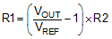
The recommended design procedure is to choose R2 = 30.1 kΩ to set the divider current at 40 μA, C1 = 15 pF for stability, and then calculate R1 using Equation 3:
Similarly, for the TPS796 (new chip), to disregard the effect of the FB pin current error term and to achieve best accuracy, choose R2 to be equal to or smaller than 550 kΩ so that the current flowing through R1 and R2 is at least five times larger than the IFB current listed in the Electrical Characteristics table. Lowering the value of R2 increases the immunity against noise injection. Increasing the value of R2 reduces the quiescent current for achieving higher efficiency at low load currents. Equation 4 calculates the setting that provides the maximum feedback divider series resistance.