SBVS360A February   2020  – November 2020 TPS7B85-Q1

PRODUCTION DATA  

  1. Features
  2. Applications
  3. Description
  4. Revision History
  5. Pin Configuration and Functions
  6. Specifications
    1. 6.1 Absolute Maximum Ratings
    2. 6.2 ESD Ratings
    3. 6.3 Recommended Operating Conditions
    4. 6.4 Thermal Information
    5. 6.5 Electrical Characteristics
    6. 6.6 Switching Characteristics
    7. 6.7 Typical Characteristics
  7. Detailed Description
    1. 7.1 Overview
    2. 7.2 Functional Block Diagram
    3. 7.3 Feature Description
      1. 7.3.1 Enable (EN)
      2. 7.3.2 Power-Good (PG)
        1. 7.3.2.1 Adjustable Power-Good (PGADJ)
      3. 7.3.3 Adjustable Power-Good Delay Timer (DELAY)
      4. 7.3.4 Sense Comparator
      5. 7.3.5 Undervoltage Lockout
      6. 7.3.6 Thermal Shutdown
      7. 7.3.7 Current Limit
    4. 7.4 Device Functional Modes
      1. 7.4.1 Device Functional Mode Comparison
      2. 7.4.2 Normal Operation
      3. 7.4.3 Dropout Operation
      4. 7.4.4 Disabled
  8. Application and Implementation
    1. 8.1 Application Information
      1. 8.1.1 Input and Output Capacitor Selection
      2. 8.1.2 Dropout Voltage
      3. 8.1.3 Reverse Current
      4. 8.1.4 Power Dissipation (PD)
        1. 8.1.4.1 Thermal Performance Versus Copper Area
      5. 8.1.5 Estimating Junction Temperature
      6. 8.1.6 SI Pin
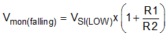
        1. 8.1.6.1 Calculating the Sense Input (SI) Pin Threshold
        2. 8.1.6.2 Different Uses for the Sense Input Pin
          1. 8.1.6.2.1 Monitoring Input Voltage
          2. 8.1.6.2.2 Creating OV and UV Power-Good
          3. 8.1.6.2.3 Monitoring a Separate Supply Voltage
      7. 8.1.7 Pulling Up the SO and PG Pins to a Different Voltage
      8. 8.1.8 Power-Good
        1. 8.1.8.1 Setting the Adjustable Power-Good Threshold
        2. 8.1.8.2 Setting the Adjustable Power-Good Delay
    2. 8.2 Typical Application
      1. 8.2.1 Design Requirements
      2. 8.2.2 Detailed Design Procedure
        1. 8.2.2.1 Input Capacitor
        2. 8.2.2.2 Output Capacitor
      3. 8.2.3 Application Curves
  9. Power Supply Recommendations
  10. 10Layout
    1. 10.1 Layout Guidelines
      1. 10.1.1 Package Mounting
      2. 10.1.2 Board Layout Recommendations to Improve PSRR and Noise Performance
    2. 10.2 Layout Example
  11. 11Device and Documentation Support
    1. 11.1 Device Support
      1. 11.1.1 Device Nomenclature
    2. 11.2 Receiving Notification of Documentation Updates
    3. 11.3 Support Resources
    4. 11.4 Trademarks
    5. 11.5 Electrostatic Discharge Caution
    6. 11.6 Glossary

Package Options

Mechanical Data (Package|Pins)
Thermal pad, mechanical data (Package|Pins)
Orderable Information

Calculating the Sense Input (SI) Pin Threshold

To use the SI pin, connect this pin to the rail being monitored through a resistor divider. This input can be configured as an undervoltage supervisor that can monitor voltage rails greater than 1.2 V or used as an overvoltage supervisor with an inverted output. Table 8-1 lists typical 1% resistor values for undervoltage monitoring where the trip point is a 5% threshold. The resistor values can be scaled to decrease the amount of current flowing through the resistor divider, but increasing the resistor values also decreases the accuracy of the resistor divider. General practice is for the current flowing through the resistor divider to be 100 times greater than the current going into the SI pin. This practice ensures the highest possible accuracy. Equation 6 can be used to calculate the resistors required in the resistor divider for any desired falling threshold. Figure 8-4 depicts the typical timing for this comparator and Figure 8-5 illustrates a block diagram for the adjustable operation.

Equation 6. GUID-532E699A-13DB-41A0-A7CE-4DDD6F037BF4-low.gif
Table 8-1 SI Resistor Divider Values
INPUT VOLTAGE (V) 5% THRESHOLD
R1 (kΩ) R2 (kΩ) THRESHOLD VOLTAGE (V)
3.3 18.2 10 3.13
5 32.4 10 4.71
6 41.2 10 5.68
7 49.9 10 6.65
8 59 10 7.66
9 66.5 10 8.49
10 75.5 10 9.49
11 80.6 10 10.06
12 93.1 10 11.44
13.5 105 10 12.77
GUID-E3ABCA10-97C8-4DE9-8954-E22408C80899-low.gifFigure 8-4 SI Timing Diagram
GUID-2E21A437-3686-4FC8-A9B4-550B3D8449D4-low.gifFigure 8-5 SI Basic Block Diagram