SLVSAZ9D June 2012 – February 2018 TPS81256
PRODUCTION DATA.
- 1 Features
- 2 Applications
- 3 Description
- 4 Revision History
- 5 Device Options
- 6 Pin Configuration and Functions
- 7 Specifications
- 8 Detailed Description
- 9 Application and Implementation
- 10Power Supply Recommendations
- 11Layout
- 12Device and Documentation Support
- 13Mechanical, Packaging, and Orderable Information
Package Options
Refer to the PDF data sheet for device specific package drawings
Mechanical Data (Package|Pins)
- SIP|9
Thermal pad, mechanical data (Package|Pins)
Orderable Information
7.6 Typical Characteristics
Table 1. Table of Graphs
| FIGURE | |||
|---|---|---|---|
| η | Efficiency | vs Output current | Figure 1, Figure 3 |
| vs Input voltage | Figure 2 | ||
| VO | DC output voltage | vs Output current | Figure 4, Figure 5, Figure 6 |
| vs Input voltage | Figure 7 | ||
| IO | Maximum output current | vs Input voltage | Figure 8 |
| ΔVO | Peak-to-peak output ripple voltage | vs Output current | Figure 8 |
| ICC | Supply current | vs Input voltage | Figure 10 |
| ILIM | Input current | vs Output current | Figure 11 |
Table 2. Table of Animated Performance Characteristics
| VIDEO | |||
|---|---|---|---|
| AC Load Response | vs. Input Voltage | Video 1 | |
| Load Transient Response (10mA to 400mA) | vs. Input Voltage | Video 2 | |
| Load Transient Response (to 400mA) | vs. Base Load Current (2.9VIN) | Video 3 | |
| vs. Base Load Current (3.6VIN) | Video 4 | ||
| vs. Base Load Current (4.2VIN) | Video 5 | ||
| Start-Up Response | vs. Delay to Load Current (2.9VIN) | Video 6 | |
| vs. Delay to Load Current (3.6VIN) | Video 7 | ||
| vs. Delay to Load Current (4.2VIN) | Video 8 | ||
| Start-Up Response (200mA IOUT) | vs. Input Voltage | Video 9 | |
| Overload Response | vs. Input Voltage | Video 10 | |
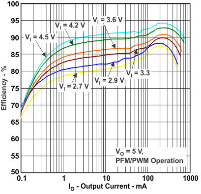 Figure 1. Efficiency vs Output Current
 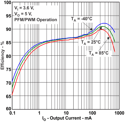 Figure 3. Efficiency vs Output Current
 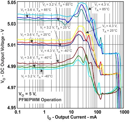 Figure 5. DC Output Voltage vs Output Current
 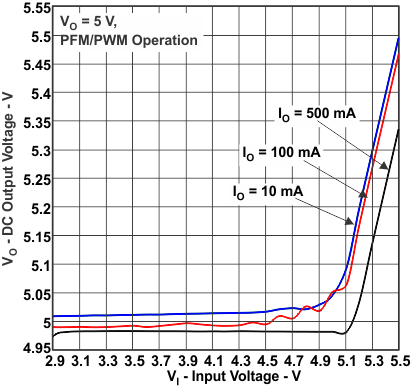 Figure 7. DC Output Voltage vs Input Voltage
 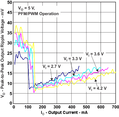 Figure 9. Peak-To-Peak Output Ripple Voltage vs Output Current
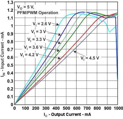
Figure 11. Input Current vs Output Current
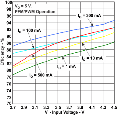 Figure 2. Efficiency vs Input Voltage
 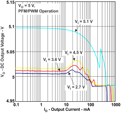 Figure 4. DC Output Voltage vs Output Current
 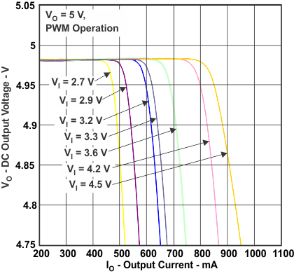 Figure 6. DC Output Voltage vs Output Current
 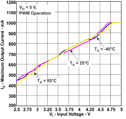 Figure 8. Maximum Output Current vs Input Voltage
 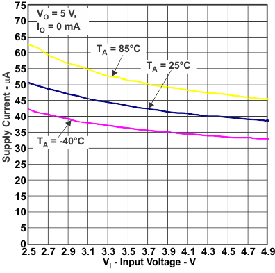 Figure 10. Supply Current vs Input Voltage