SLUSAN7C SEPTEMBER 2011 – April 2018 TPS84210
PRODUCTION DATA.
- 1 Features
- 2 Applications
- 3 Description
- 4 Revision History
- 5 Pin Configuration and Functions
- 6 Specifications
- 7 Functional Block Diagram
- 8 Application and Implementation
- 9 Capacitor Recommendations For The TPS84210 Power Supply
- 10Transient Response
- 11Application Schematics
- 12Power Good (PWRGD)
- 13Power-Up Characteristics
- 14Remote Sense
- 15Output On/Off Inhibit (INH)
- 16Slow Start (SS/TR)
- 17Overcurrent Protection
- 18Synchronization (CLK)
- 19Sequencing (SS/TR)
- 20Programmable Undervoltage Lockout (UVLO)
- 21Thermal Shutdown
- 22Layout Guidelines
- 23Layout Example
- 24EMI
- 25Device and Documentation Support
- 26Mechanical, Packaging, and Orderable Information
Package Options
Refer to the PDF data sheet for device specific package drawings
Mechanical Data (Package|Pins)
- RKG|39
Thermal pad, mechanical data (Package|Pins)
Orderable Information
19 Sequencing (SS/TR)
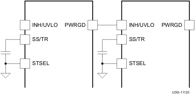
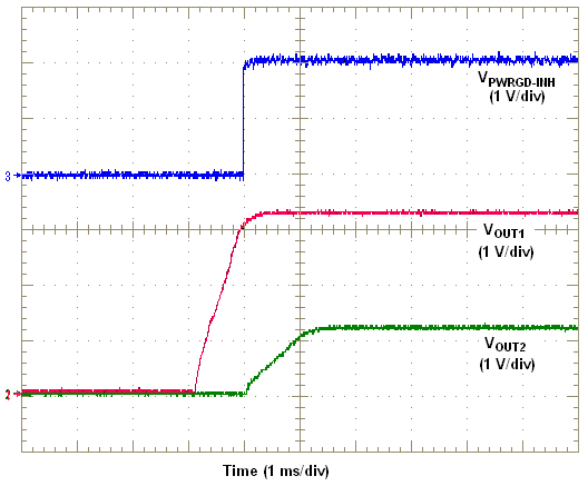
Many of the common power supply sequencing methods can be implemented using the SS/TR, INH and PWRGD pins. The sequential method is illustrated in Figure 29 using two TPS84210 devices. The PWRGD pin of the first device is coupled to the INH pin of the second device which enables the second power supply once the primary supply reaches regulation. Do not place a pull-up resistor on PWRGD in this configuration. Figure 30 shows sequential turn-on waveforms of two TPS84210 devices.
 Figure 29. Sequencing Schematic
  Figure 30. Sequencing Waveforms
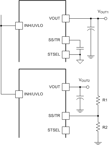
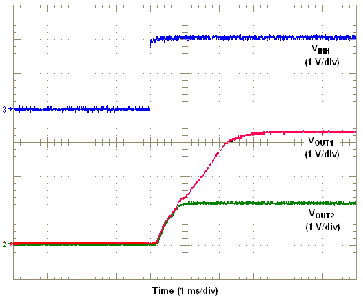
 Simultaneous power supply sequencing can be implemented by connecting the resistor network of R1 and R2 shown in Figure 31 to the output of the power supply that needs to be tracked or to another voltage reference source. Figure 32 shows simultaneous turn-on waveforms of two TPS84210 devices. Use and to calculate the values of R1 and R2.
 Figure 31. Simultaneous Tracking Schematic
  Figure 32. Simultaneous Tracking Waveforms