SLUSAN7C SEPTEMBER 2011 – April 2018 TPS84210
PRODUCTION DATA.
- 1 Features
- 2 Applications
- 3 Description
- 4 Revision History
- 5 Pin Configuration and Functions
- 6 Specifications
- 7 Functional Block Diagram
- 8 Application and Implementation
- 9 Capacitor Recommendations For The TPS84210 Power Supply
- 10Transient Response
- 11Application Schematics
- 12Power Good (PWRGD)
- 13Power-Up Characteristics
- 14Remote Sense
- 15Output On/Off Inhibit (INH)
- 16Slow Start (SS/TR)
- 17Overcurrent Protection
- 18Synchronization (CLK)
- 19Sequencing (SS/TR)
- 20Programmable Undervoltage Lockout (UVLO)
- 21Thermal Shutdown
- 22Layout Guidelines
- 23Layout Example
- 24EMI
- 25Device and Documentation Support
- 26Mechanical, Packaging, and Orderable Information
Package Options
Refer to the PDF data sheet for device specific package drawings
Mechanical Data (Package|Pins)
- RKG|39
Thermal pad, mechanical data (Package|Pins)
Orderable Information
10 Transient Response
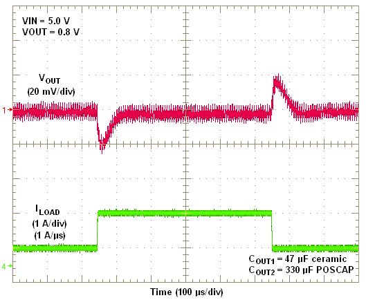 Figure 11. VIN = 5 V, VOUT = 0.8 V, 1 A Load Step
 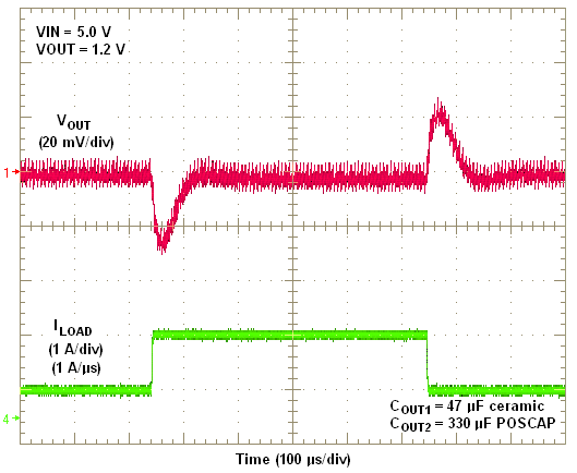 Figure 13. VIN = 5V, VOUT = 1.2V, 1A Load Step
 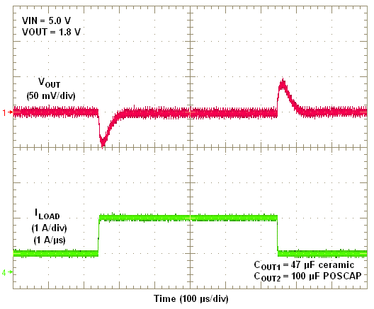 Figure 15. VIN = 5V, VOUT = 1.8V, 1A Load Step
 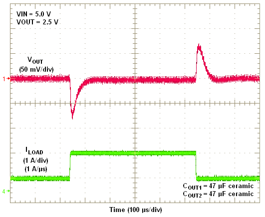 Figure 17. VIN = 5V, VOUT = 2.5V, 1A Load Step
 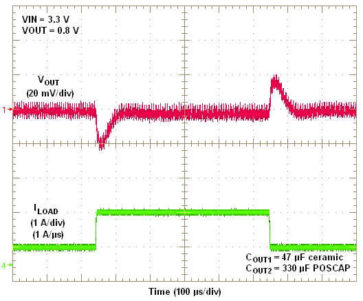 Figure 12. VIN = 3.3 V, VOUT = 0.8 V, 1 A Load Step
 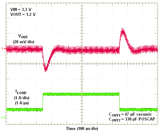 Figure 14. VIN = 3.3V, VOUT = 1.2V, 1A Load Step
 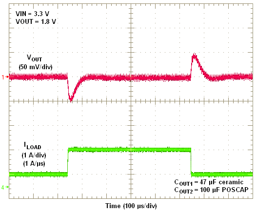 Figure 16. VIN = 3.3V, VOUT = 1.8V, 1A Load Step
 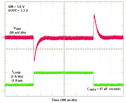 Figure 18. VIN = 5V, VOUT = 3.3V, 1A Load Step