SNVS901A March 2014 – May 2014 TPS92511
PRODUCTION DATA.
- 1 Features
- 2 Applications
- 3 Description
- 4 Revision History
- 5 Pin Configuration and Functions
- 6 Specifications
-
7 Detailed Description
- 7.1 Overview
- 7.2 Functional Block Diagram
- 7.3
Feature Description
- 7.3.1 Pulse Level Modulation (PLM) Control
- 7.3.2 Pulse Level Modulation (PLM) Operaion Principles
- 7.3.3 PLM Control enable Common-Anode Low-Side Sensing (CALS)Technique to Save Wiring
- 7.3.4 Internal Regulator
- 7.3.5 Setting The Switching Frequency
- 7.3.6 Setting The LED Current
- 7.3.7 Integrated MOSFET
- 7.3.8 Inductor Selection
- 7.3.9 Integrated MOSFET Current Limit
- 7.3.10 PWM Dimming Control
- 7.3.11 Analog Dimming
- 7.3.12 High Voltage Buck Configuration
- 7.3.13 Thermal Foldback
- 7.3.14 EMI Consideration
- 7.4 Device Functional Modes
- 8 Application and Implementation
- 9 Power Supply Recommendation
- 10Layout
- 11Device and Documentation Support
- 12Mechanical, Packaging, and Orderable Information
Package Options
Mechanical Data (Package|Pins)
- DDA|8
Thermal pad, mechanical data (Package|Pins)
- DDA|8
Orderable Information
5 Pin Configuration and Functions
DDA (SO THERMAL PAD) PACKAGE
8 PINS
(TOP VIEW)
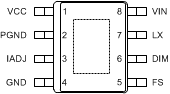
Pin Functions
| PIN | DESCRIPTION | |
|---|---|---|
| NAME | NO. | |
| DIM | 6 | PWM Dimming Control. Apply logic level PWM signal to this pin dims the LED string. This pin is internally pulled up. |
| FS | 5 | Switching Frequency Setting. An external resistor RFS connecting the FS pin to ground programs the switching frequency from 50 kHz to 500 kHz. |
| GND | 4 | Analog Signal Ground. |
| IADJ | 3 | Average LED Current Setting. An external resistor RIADJ connecting the IADJ pin to ground programs the average LED current. |
| LX | 7 | Integrated MOSFET Drain. Internally connected to the drain of the integrated MOSFET. Connect this pin to the output inductor and anode of the Schottky diode. |
| PGND | 2 | Power Ground. Must be connected to the GND pin for normal operation. The PGND and GND pins are not internally shorted. |
| VCC | 1 | Internal Regulator Output. Typically regulated to 5.4 V. Connect a capacitor of larger than 1 µF between the VCC and GND pins. |
| VIN | 8 | Input Voltage. Supply pin to the device. The input voltage range is from 4.5 V to 65 V. |
| Thermal pad | Thermal Connection Pad. Connect to a ground plane for heat dissipation. | |