SNVS901A March 2014 – May 2014 TPS92511
PRODUCTION DATA.
- 1 Features
- 2 Applications
- 3 Description
- 4 Revision History
- 5 Pin Configuration and Functions
- 6 Specifications
-
7 Detailed Description
- 7.1 Overview
- 7.2 Functional Block Diagram
- 7.3
Feature Description
- 7.3.1 Pulse Level Modulation (PLM) Control
- 7.3.2 Pulse Level Modulation (PLM) Operaion Principles
- 7.3.3 PLM Control enable Common-Anode Low-Side Sensing (CALS)Technique to Save Wiring
- 7.3.4 Internal Regulator
- 7.3.5 Setting The Switching Frequency
- 7.3.6 Setting The LED Current
- 7.3.7 Integrated MOSFET
- 7.3.8 Inductor Selection
- 7.3.9 Integrated MOSFET Current Limit
- 7.3.10 PWM Dimming Control
- 7.3.11 Analog Dimming
- 7.3.12 High Voltage Buck Configuration
- 7.3.13 Thermal Foldback
- 7.3.14 EMI Consideration
- 7.4 Device Functional Modes
- 8 Application and Implementation
- 9 Power Supply Recommendation
- 10Layout
- 11Device and Documentation Support
- 12Mechanical, Packaging, and Orderable Information
Package Options
Mechanical Data (Package|Pins)
- DDA|8
Thermal pad, mechanical data (Package|Pins)
- DDA|8
Orderable Information
6 Specifications
6.1 Absolute Maximum Ratings (1)
Unless otherwise specified, TJ = TA = 25°C| MIN | NOM | MAX | UNIT | ||
|---|---|---|---|---|---|
| Pin voltage range | VIN to GND | –0.3 | 65 | V | |
| VIN to GND (Transient) | –0.3 | 67 | V | ||
| LX to PGND | –0.3 | 65 | V | ||
| LX to PGND (Transient) | –3(2ns) | 67 | V | ||
| FS, IADJ to GND | –0.3 | 5 | V | ||
| DIM to GND | –0.3 | 6 | V | ||
| VCC to GND | –0.3 | 7 | V | ||
| Temperature range | Operating junction temperature range, TJ | –40 | Internally limited | °C |
(1) Absolute Maximum Ratings are limits beyond which damage to the device may occur. Operating Ratings are conditions under which operation of the device is intended to be functional. For specified specifications and test conditions, see the Electrical Characteristics.
6.2 Handling Ratings
| MIN | MAX | UNIT | ||
|---|---|---|---|---|
| Tstg | Storage temperature range | -65 | 150 | °C |
| VESD(1) | Human Body Model (HBM) ESD stress voltage (2) | 1.5 | kV | |
| Charged Device Model (CDM) ESD stress voltage(3) | 1.5 | kV |
(1) Electrostatic discharge (ESD) to measure device sensitivity and immunity to damage caused by assembly line electrostatic discharges in to the device.
(2) Level listed above is the passing level per ANSI, ESDA, and JEDEC JS-001. JEDEC document JEP155 states that 500-V HBM allows safe manufacturing with a standard ESD control process.
(3) Level listed above is the passing level per EIA-JEDEC JESD22-C101. JEDEC document JEP157 states that 250-V CDM allows safe manufacturing with a standard ESD control process.
6.3 Recommended Operating Conditions
| MIN | NOM | MAX | UNIT | ||
|---|---|---|---|---|---|
| VIN | Supply voltage range | 4.5 | 65 | V | |
| TA | Operating free air temperature | –40 | 125 | °C | |
| TJ | Operating junction temperature | -40 | 125 | °C | |
6.4 Thermal Information
| THERMAL METRIC(1) | TPS92511 | UNIT | |
|---|---|---|---|
| DDA | |||
| 8 PINS | |||
| RθJA | Junction-to-ambient thermal resistance | 59.9 | °C/W |
| RθJCtop | Junction-to-case (top) thermal resistance | 59.1 | |
| RθJB | Junction-to-board thermal resistance | 30.6 | |
| ψJT | Junction-to-top characterization parameter | 11.0 | |
| ψJB | Junction-to-board characterization parameter | 30.5 | |
| RθJCbot | Junction-to-case (bottom) thermal resistance | 4.2 | |
(1) For more information about traditional and new thermal metrics, see the IC Package Thermal Metrics application report, SPRA953.
6.5 Electrical Characteristics
Unless otherwise specified, -40°C ≤ TJ = TA ≤ 125°C, VIN = 48 V| PARAMETER | CONDITIONS | MIN | TYP | MAX | UNIT | |
|---|---|---|---|---|---|---|
| SYSTEM | ||||||
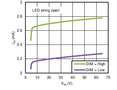
| IIN-DIM-HIGH | VIN Operating Current | 4.5 V ≤ VIN ≤ 65 V, RIADJ = 3 kΩ, VDIM = High | 2.8 | 3.15 | mA | |
| IIN-DIM-LOW | VIN Standby Current | 4.5 V ≤ VIN ≤ 65 V, RIADJ = 3 kΩ, VDIM = Low | 2.3 | 2.7 | mA | |
| ILX-OFF | LX Pin Current | Main switch turned OFF, VLX = VIN = 65 V | 0.1 | 1.0 | µA | |
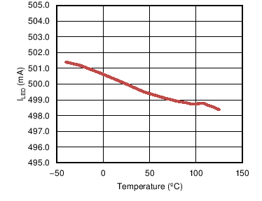
| ILED | Average LED Current | VFS = 4.6V, RIADJ = 3 kΩ, TA = 25°C | 484 | 502 | 520 | mA |
| VFS = 4.6V, RIADJ = 3 kΩ | 477 | 502 | 528 | mA | ||
| VFS = 4.6V, RIADJ = 6 kΩ, TA = 25°C | 236 | 249 | 262 | mA | ||
| VFS = 4.6V, RIADJ = 6 kΩ | 233 | 249 | 268 | mA | ||
| VFS = 4.6V, RIADJ = 10 kΩ, TA = 25°C | 138 | 149 | 160 | mA | ||
| VFS = 4.6V, RIADJ = 10 kΩ | 133 | 149 | 166 | mA | ||
| VIADJ | IADJ Pin voltage | 1.224 | 1.25 | 1.278 | V | |
| VDIM-ON | DIM Pin Upper Threshold | VDIM Increasing | 0.85 | 1.0 | 1.25 | V |
| VDIM-OFF | DIM Pin Lower Threshold | VDIM Decreasing | 0.44 | V | ||
| VDIM-HYS | DIM Pin Threshold Hysteresis | 325 | mV | |||
| fSW | Switching frequency | RFS = 20 kΩ | 450 | 500 | 550 | kHz |
| ton(min) | Minimum On-time | 250 | 400 | ns | ||
| INTERNAL REGULATOR | ||||||
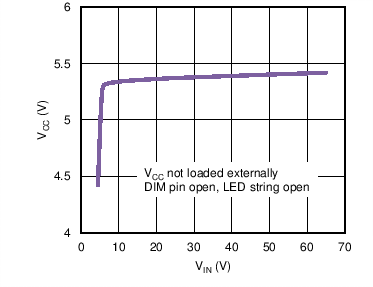
| VCC | VCC Regulated Output Voltage | CVCC =1 µF, no load | 4.7 | 5.4 | 6.0 | V |
| CVCC =1 µF, VIN = 4.5V, 2 mA load | 3.7 | 4.1 | V | |||
| VCC-UVLO-ON | VCC UVLO Upper Threshold | VCC rising | 3.50 | 3.75 | 4.00 | V |
| VCC-UVLO-OFF | VCC UVLO Lower Threshold | VCC falling | 3.05 | V | ||
| VCC-UVLO-HYS | VCC UVLO Hysteresis | 275 | mV | |||
| INTEGRATED MOSFET | ||||||
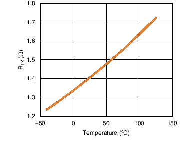
| RLX | Resistance Across LX and GND | Main Switch Turned ON, TA = 25°C | 1.4 | 2.15 | Ω | |
| THERMAL SHUTDOWN | ||||||
| TSD | Thermal shutdown temperature | TJ Rising | 165 | °C | ||
| TSD-HYS | Thermal shutdown hysteresis | TJ Falling | 10 | |||
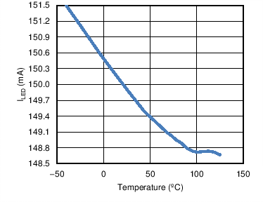
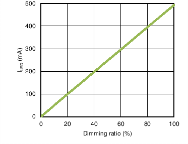
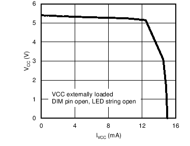
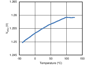
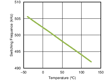
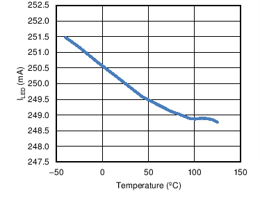
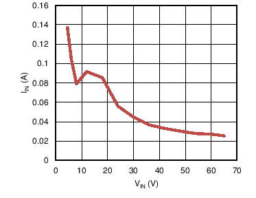
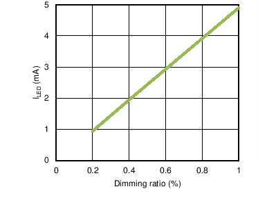
6.6 Typical Characteristics
Unless otherwise specified, all curves are taken at VIN = 48V with configuration in the application circuit for driving 12 LEDs with ILED = 0.5A and fSW = 300 kHz as shown in this datasheet, and TA = 25°C.