SNVS901A March 2014 – May 2014 TPS92511
PRODUCTION DATA.
- 1 Features
- 2 Applications
- 3 Description
- 4 Revision History
- 5 Pin Configuration and Functions
- 6 Specifications
-
7 Detailed Description
- 7.1 Overview
- 7.2 Functional Block Diagram
- 7.3
Feature Description
- 7.3.1 Pulse Level Modulation (PLM) Control
- 7.3.2 Pulse Level Modulation (PLM) Operaion Principles
- 7.3.3 PLM Control enable Common-Anode Low-Side Sensing (CALS)Technique to Save Wiring
- 7.3.4 Internal Regulator
- 7.3.5 Setting The Switching Frequency
- 7.3.6 Setting The LED Current
- 7.3.7 Integrated MOSFET
- 7.3.8 Inductor Selection
- 7.3.9 Integrated MOSFET Current Limit
- 7.3.10 PWM Dimming Control
- 7.3.11 Analog Dimming
- 7.3.12 High Voltage Buck Configuration
- 7.3.13 Thermal Foldback
- 7.3.14 EMI Consideration
- 7.4 Device Functional Modes
- 8 Application and Implementation
- 9 Power Supply Recommendation
- 10Layout
- 11Device and Documentation Support
- 12Mechanical, Packaging, and Orderable Information
Package Options
Mechanical Data (Package|Pins)
- DDA|8
Thermal pad, mechanical data (Package|Pins)
- DDA|8
Orderable Information
10 Layout
10.1 Layout Guidelines
- The PCB layout of the TPS92511 application circuit plays an important role in optimizing the performance.
- The external components should be placed as close to the TPS92511 as possible to minimize resistance and parasitic inductance of copper traces.
- For example, D1 and L1 should be near the LX pin, and CVCC should be near the VCC pin, and the connecting copper traces are short and thick.
- The exposed pad of the TPS92511, which is internally connected to the die substrate, should be connect to a ground plane, and the plane should be extended as much as possible on the same copper layer around the TPS92511.
- Using numerous vias beneath the exposed pad to dissipate heat to another copper layer is also a good practice.
10.2 Layout Example
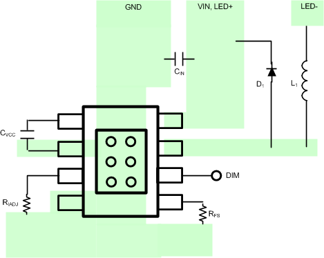 Figure 32. TPS92511 Board Layout
10.2.1 Thermal Consideration
ΨJT (shown in session 6.4 Thermal Information) is a relatively small value for package with exposed pad since most of the heat is dissipated through the exposed pad to the copper plate of the PCB (assuming optimized PCB layout), relatively little heat goes to the top of the device. The top of the device mold compound temperature is physically close to the device junction temperature.
For example, a 30W output TPS92511 end system at 95% power efficiency (can be estimated from the efficiency curves of Figure 13), power loss is 1.6W. Assuming all the heat is generated from the TPS92511 (which is true for high VLED), and assuming half of the heat generated is dissipated through the top of the device. Now ΨJT is 11 °C/W, the device junction temperature is estimated to be higher than the package’s top-surface temperature by 11 x 1.6 x 0.5 = 8.8 (°C). If the package top-surface temperature is measured to be 90 °C (for example by an IR camera), the device junction temperature is around 99 °C, which is within the 125°C maximum junction temperature requirement with margin.