SLVSG60A April 2023 – April 2024 TPS929160-Q1
PRODUCTION DATA
- 1
- 1 Features
- 2 Applications
- 3 Description
- 4 Pin Configuration and Functions
- 5 Specifications
-
6 Detailed Description
- 6.1 Overview
- 6.2 Functional Block Diagram
- 6.3
Feature Description
- 6.3.1 Device Bias and Power
- 6.3.2 Constant Current Output
- 6.3.3 PWM Dimming
- 6.3.4 FAIL-SAFE State Operation
- 6.3.5 On-Chip, 8-Bit, Analog-to-Digital Converter (ADC)
- 6.3.6 NSTB Output
- 6.3.7
Diagnostic and Protection in NORMAL State
- 6.3.7.1 VBAT Undervoltage Lockout Diagnostics in NORMAL state
- 6.3.7.2 Low-Supply Warning Diagnostics in NORMAL State
- 6.3.7.3 Supply Undervoltage Diagnostics in NORMAL State
- 6.3.7.4 Reference Diagnostics in NORMAL state
- 6.3.7.5 Pre-Thermal Warning in NORMAL state
- 6.3.7.6 Overtemperature Protection in NORMAL state
- 6.3.7.7 Overtemperature Shutdown in NORMAL state
- 6.3.7.8 LED Open-Circuit Diagnostics in NORMAL state
- 6.3.7.9 LED Short-Circuit Diagnostics in NORMAL state
- 6.3.7.10 Single-LED Short-Circuit Detection in NORMAL state
- 6.3.7.11 EEPROM CRC Error in NORMAL state
- 6.3.7.12 Communication Loss Diagnostic in NORMAL state
- 6.3.7.13 Fault Masking in NORMAL state
- 55
- 6.3.8
Diagnostic and Protection in FAIL-SAFE states
- 6.3.8.1 Supply Undervoltage Lockout Diagnostics in FAIL-SAFE states
- 6.3.8.2 Low-Supply Warning Diagnostics in FAIL-SAFE states
- 6.3.8.3 Supply Undervoltage Diagnostics in FAIL-SAFE State
- 6.3.8.4 Reference Diagnostics in FAIL-SAFE states
- 6.3.8.5 Pre-Thermal Warning in FAIL-SAFE state
- 6.3.8.6 Overtemperature Protection in FAIL-SAFE state
- 6.3.8.7 Overtemperature Shutdown in FAIL-SAFE state
- 6.3.8.8 LED Open-Circuit Diagnostics in FAIL-SAFE state
- 6.3.8.9 LED Short-Circuit Diagnostics in FAIL-SAFE state
- 6.3.8.10 Single-LED Short-Circuit Detection in FAIL-SAFE state
- 6.3.8.11 EEPROM CRC Error in FAIL-SAFE state
- 6.3.8.12 Fault Masking in FAIL-SAFE state
- 69
- 6.3.9 OFAF Setup In FAIL-SAFE state
- 6.3.10 ERR Output
- 6.4 Device Functional Modes
- 6.5 Programming
- 6.6 Register Maps
- 7 Application and Implementation
- 8 Device and Documentation Support
- 9 Revision History
- 10Mechanical, Packaging, and Orderable Information
Package Options
Refer to the PDF data sheet for device specific package drawings
Mechanical Data (Package|Pins)
- DCP|38
Thermal pad, mechanical data (Package|Pins)
- DCP|38
Orderable Information
6.3.3.5 Linear Brightness Control
When register EXPEN is set to 0, the MSB 8 bits of 12-bit binary input to PWM generator are directly copied from 8-bit register PWMOUTXn, and the LSB 4 bits are directly copied from 4-bit register PWMLOWOUTXn. The PWM output duty cycle can be calculated with the following equation. The PWM output duty cycle is linearly controlled by the register PWMOUTXn and PWMLOWOUTXn, which provides the linear brightness control to each channel output. When PWMOUTXn is FFh, and PWMLOWOUTXn is Fh, the duty cycle is 100% exceptionally.
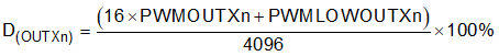
where
- PWMOUTXn is decimal number from 0 to 255.
- PWMLOWOUTXn is decimal number from 0 to 15.
- X is from A to H, n is 0 or 1 for different output channel.
Because the 12-bit PWM duty cycles require 2 bytes of write operation to update the completed data, the output PWM duty cycle is not changed in between of the two bytes data transmission. TPS929160-Q1 only updates PWM duty cycle of any output when its high 8-bit PWMOUTXn is written. When very fast brightness change is needed, for example, fade-in and fade-out effects, simultaneous PWM duty cycle change of all channels is required. Setting SHAREPWM to 1 enables all channels using the PWM duty cycle setting of channel A0 to save communication latency. When disabling the SHAREPWM, PWM outputs of all the channels remain unchanged until the corresponding PWM duty cycle setting registers are modified.
To reduce the data transmission for large quantity of the LED pixel control, 8-bit PWM duty cyle resolution can be adopted by writing 0 to 12BIT in DIM register. The master only needs to update high 8-bit PWMOUTXn register to change the brightness of target output channel. The low 4-bit registers PWMLOWOUTXn are ignored. The PWM duty-cycle calculation is shown in he below equation. When PWMOUTXn is FFh, the duty cycle is 100% exceptionally.
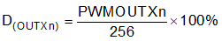
where
- PWMOUTXn is decimal number from 0 to 255.
- X is from A to H, n is 0 or 1 for different output channel.