SLVSG60A April 2023 – April 2024 TPS929160-Q1
PRODUCTION DATA
- 1
- 1 Features
- 2 Applications
- 3 Description
- 4 Pin Configuration and Functions
- 5 Specifications
-
6 Detailed Description
- 6.1 Overview
- 6.2 Functional Block Diagram
- 6.3
Feature Description
- 6.3.1 Device Bias and Power
- 6.3.2 Constant Current Output
- 6.3.3 PWM Dimming
- 6.3.4 FAIL-SAFE State Operation
- 6.3.5 On-Chip, 8-Bit, Analog-to-Digital Converter (ADC)
- 6.3.6 NSTB Output
- 6.3.7
Diagnostic and Protection in NORMAL State
- 6.3.7.1 VBAT Undervoltage Lockout Diagnostics in NORMAL state
- 6.3.7.2 Low-Supply Warning Diagnostics in NORMAL State
- 6.3.7.3 Supply Undervoltage Diagnostics in NORMAL State
- 6.3.7.4 Reference Diagnostics in NORMAL state
- 6.3.7.5 Pre-Thermal Warning in NORMAL state
- 6.3.7.6 Overtemperature Protection in NORMAL state
- 6.3.7.7 Overtemperature Shutdown in NORMAL state
- 6.3.7.8 LED Open-Circuit Diagnostics in NORMAL state
- 6.3.7.9 LED Short-Circuit Diagnostics in NORMAL state
- 6.3.7.10 Single-LED Short-Circuit Detection in NORMAL state
- 6.3.7.11 EEPROM CRC Error in NORMAL state
- 6.3.7.12 Communication Loss Diagnostic in NORMAL state
- 6.3.7.13 Fault Masking in NORMAL state
- 55
- 6.3.8
Diagnostic and Protection in FAIL-SAFE states
- 6.3.8.1 Supply Undervoltage Lockout Diagnostics in FAIL-SAFE states
- 6.3.8.2 Low-Supply Warning Diagnostics in FAIL-SAFE states
- 6.3.8.3 Supply Undervoltage Diagnostics in FAIL-SAFE State
- 6.3.8.4 Reference Diagnostics in FAIL-SAFE states
- 6.3.8.5 Pre-Thermal Warning in FAIL-SAFE state
- 6.3.8.6 Overtemperature Protection in FAIL-SAFE state
- 6.3.8.7 Overtemperature Shutdown in FAIL-SAFE state
- 6.3.8.8 LED Open-Circuit Diagnostics in FAIL-SAFE state
- 6.3.8.9 LED Short-Circuit Diagnostics in FAIL-SAFE state
- 6.3.8.10 Single-LED Short-Circuit Detection in FAIL-SAFE state
- 6.3.8.11 EEPROM CRC Error in FAIL-SAFE state
- 6.3.8.12 Fault Masking in FAIL-SAFE state
- 69
- 6.3.9 OFAF Setup In FAIL-SAFE state
- 6.3.10 ERR Output
- 6.4 Device Functional Modes
- 6.5 Programming
- 6.6 Register Maps
- 7 Application and Implementation
- 8 Device and Documentation Support
- 9 Revision History
- 10Mechanical, Packaging, and Orderable Information
Package Options
Refer to the PDF data sheet for device specific package drawings
Mechanical Data (Package|Pins)
- DCP|38
Thermal pad, mechanical data (Package|Pins)
- DCP|38
Orderable Information
6.3.6 NSTB Output
The TPS929160-Q1 device provides a NSTB output to control external CAN transciever enter into sleep mode. The NSTB ouput is an open drain structure with internal pulling up path to VLDO, and it is recommended to be pulled down to GND through an external 100kΩ resistor. The internal pull up of NSTB output is turned on by default and only turned off when NSTB register is set to 1h. The pulling up path is turned on again when the NSTB register is set to 0h. Which means that the NSTB output always exhibits VLDO voltage output after device is enabled by pulling high EN pin, and it goes to low once the NSTB register is set to 1h or the TPS929160-Q1 is disabled.
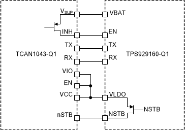
With this NSTB output, the TPS929160-Q1 can set an external CAN transciever such as TCAN1043-Q1 into sleep mode by controlling the nSTB input pin of TCAN1043-Q1 to minimize the power consumption. The TCAN1043-Q1 can also remove the pulling up of the EN pin of TPS929160-Q1 by its INH output to shutdown the TPS929160-Q1 after entering the sleep mode. The TCAN1043-Q1 can be waked up again by a specified WUP pattern and release INH output to turn on the TPS929160-Q1 as well. Figure 6-7 and Figure 6-8 are the typical application and timing diagram for TPS929160-Q1 cooperating with TCAN1043-Q1 to achieve the low current consumption in sleep mode.
 Figure 6-7 Sleep Mode Typical Application Diagram
 Figure 6-8 Sleep Mode Access and Exit
Timing Diagram