SCDS324E August 2011 – Oct 2019 TS3DS10224
PRODUCTION DATA.
- 1 Features
- 2 Applications
- 3 Description
- 4 Revision History
- 5 Pin Configuration and Functions
-
6 Specifications
- 6.1 Absolute Maximum Ratings
- 6.2 ESD Ratings
- 6.3 Recommended Operating Conditions
- 6.4 Thermal Information
- 6.5 Electrical Characteristics: Differential 1:4 or 2‑Channel 1:2 Configurations
- 6.6 Electrical Characteristics: Fan-Out 1:2 Configurations
- 6.7 Switching Characteristics: Differential 1:4 or 2‑Channel 1:2 Configurations
- 6.8 Switching Characteristics: Fan-Out 1:2 Configurations
- 6.9 Dynamic Characteristics: Differential 1:4 or 2‑Channel 1:2 Configurations
- 6.10 Dynamic Characteristics: Fan-Out 1:2 Configurations
- 6.11 Typical Characteristics
- 7 Parameter Measurement Information
- 8 Detailed Description
- 9 Application and Implementation
- 10Power Supply Recommendations
- 11Layout
- 12Device and Documentation Support
- 13Mechanical, Packaging, and Orderable Information
Package Options
Refer to the PDF data sheet for device specific package drawings
Mechanical Data (Package|Pins)
- RUK|20
Thermal pad, mechanical data (Package|Pins)
- RUK|20
Orderable Information
8.4.2 Differential Crosspoint Switch
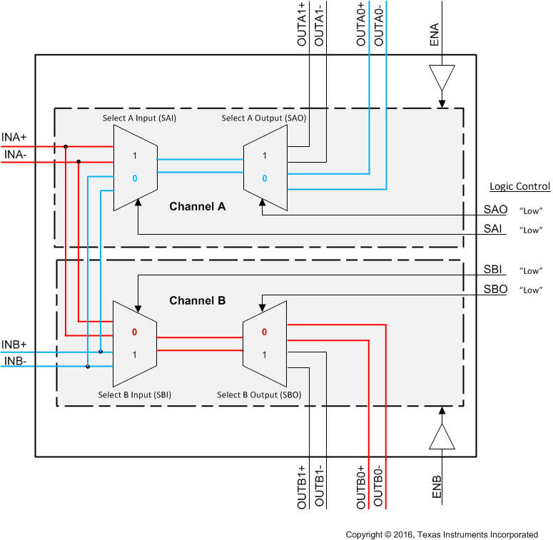
The TS3DS10224 can be configured as a differential crosspoint switch. Crosspoint switches are particularly helpful when traces have to cross in simplifying layouts, and when switching the top and bottom signals of the reversible connector in USB Type-C applications.
Table 2 shows that the inputs INA and INB can be routed to OUTA or OUTB. This is accomplished by setting the Select A Output (SAO) and Select B Output (SBO) LOW and selecting which input goes to the output by toggling the Select A Input (SAI) and Select B Input (SBI) pins.
Table 2. Differential Crosspoint Switch Function Table
| LOGIC CONTROL SETTING | SIGNAL ROUTING | ||||
|---|---|---|---|---|---|
| SAI | SBI | SAO | SBO | INA | INB |
| 0 | 0 | 0 | 0 | OUTB0 | OUTA0 |
| 1 | 1 | 0 | 0 | OUTA0 | OUTB0 |
 Figure 14. Differential Crosspoint Switch Block Diagram