SLLSF47D February   2018  – April 2024 TUSB1044

PRODUCTION DATA  

  1.   1
  2. Features
  3. Applications
  4. Description
  5. Pin Configuration and Functions
  6. Specifications
    1. 5.1 Absolute Maximum Ratings
    2. 5.2 ESD Ratings
    3. 5.3 Recommended Operating Conditions
    4. 5.4 Thermal Information
    5. 5.5 Electrical Characteristics
    6. 5.6 Switching Characteristics
    7. 5.7 Timing Requirements
    8. 5.8 Typical Characteristics
  7. Detailed Description
    1. 6.1 Overview
    2. 6.2 Functional Block Diagram
    3. 6.3 Feature Description
      1. 6.3.1 USB 3.1
      2. 6.3.2 DisplayPort
      3. 6.3.3 4-Level Inputs
      4. 6.3.4 Receiver Linear Equalization
    4. 6.4 Device Functional Modes
      1. 6.4.1 Device Configuration in GPIO mode
      2. 6.4.2 Device Configuration in I2C Mode
      3. 6.4.3 DisplayPort Mode
      4. 6.4.4 Custom Alternate Mode
      5. 6.4.5 Linear EQ Configuration
      6. 6.4.6 Adjustable VOD Linear Range and DC Gain
      7. 6.4.7 USB3.1 Modes
    5. 6.5 Programming
      1. 6.5.1 Use The Following Procedure to Write to TUSB1044 I2C Registers:
      2. 6.5.2 Use The Following Procedure to Read the TUSB1044 I2C Registers:
      3. 6.5.3 Use The Following Procedure for Setting a Starting Sub-Address for I2C Reads:
    6. 6.6 Register Maps
      1. 6.6.1 TUSB1044 Registers
  8. Application and Implementation
    1. 7.1 Application Information
    2. 7.2 Typical Application
      1. 7.2.1 Design Requirements
      2. 7.2.2 Detailed Design Procedure
      3. 7.2.3 Application Curve
    3. 7.3 System Examples
      1. 7.3.1 USB 3.1 only (USB/DP Alternate Mode)
      2. 7.3.2 USB3.1 and 2 lanes of DisplayPort
      3. 7.3.3 DisplayPort Only
      4. 7.3.4 USB 3.1 only (USB/Custom Alternate Mode)
      5. 7.3.5 USB3.1 and 1 Lane of Custom Alt Mode
      6. 7.3.6 USB3.1 and 2 Lane of Custom Alt Mode
      7. 7.3.7 USB3.1 and 4 Lane of Custom Alt Mode
    4. 7.4 Power Supply Recommendations
    5. 7.5 Layout
      1. 7.5.1 Layout Guidelines
      2. 7.5.2 Layout Example
  9. Device and Documentation Support
    1. 8.1 Documentation Support
      1. 8.1.1 Related Documentation
    2. 8.2 Receiving Notification of Documentation Updates
    3. 8.3 Support Resources
    4. 8.4 Trademarks
    5. 8.5 Electrostatic Discharge Caution
    6. 8.6 Glossary
  10. Revision History
  11. 10Mechanical, Packaging, and Orderable Information

Package Options

Mechanical Data (Package|Pins)
Thermal pad, mechanical data (Package|Pins)
Orderable Information

Detailed Design Procedure

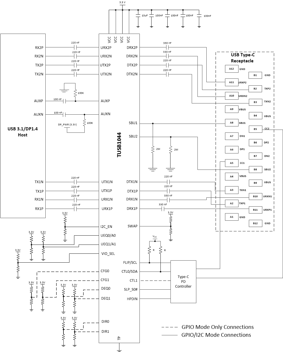
A typical usage of the TUSB1044 device is shown in Figure 7-2. The device can be controlled either through its GPIO pins or through its I2C interface. In Figure 7-2, a Type-C PD controller is used to configure the device through the I2C interface. In I2C mode, the equalization settings for each receiver can be independently controlled through I2C registers. For this reason, all of the equalization pins (UEQ[1:0] and DEQ[1:0]) can be left unconnected. If these pins are left unconnected, the TUSB1044 7-bit I2C slave address is 12h because both UEQ1/A1 and UEQ0/A0 are at pin level "F". If a different I2C slave address is desired, UEQ1/A1 and UEQ0/A0 pins should be set to a level which produces the desired I2C slave address.

Recent ECN (Engineering Change Notice) to the USB3.1 specification allows for AC-coupling capacitors between USB receptacle and the USB3.1 receiver pins of a device/host/hub. The TUSB1044 does support the additional AC-capacitor as depicted in Figure 7-2 on pins DRX2P/N and DRX1P/N. This AC-coupling capacitor should be no smaller than 297 nF. A value of 330 nF is recommended.
GUID-F5C7D7BE-9633-44EC-88C0-544F37BF07FE-low.gif Figure 7-2 Typical Application Circuit