SLLSF47D February   2018  – April 2024 TUSB1044

PRODUCTION DATA  

  1.   1
  2. Features
  3. Applications
  4. Description
  5. Pin Configuration and Functions
  6. Specifications
    1. 5.1 Absolute Maximum Ratings
    2. 5.2 ESD Ratings
    3. 5.3 Recommended Operating Conditions
    4. 5.4 Thermal Information
    5. 5.5 Electrical Characteristics
    6. 5.6 Switching Characteristics
    7. 5.7 Timing Requirements
    8. 5.8 Typical Characteristics
  7. Detailed Description
    1. 6.1 Overview
    2. 6.2 Functional Block Diagram
    3. 6.3 Feature Description
      1. 6.3.1 USB 3.1
      2. 6.3.2 DisplayPort
      3. 6.3.3 4-Level Inputs
      4. 6.3.4 Receiver Linear Equalization
    4. 6.4 Device Functional Modes
      1. 6.4.1 Device Configuration in GPIO mode
      2. 6.4.2 Device Configuration in I2C Mode
      3. 6.4.3 DisplayPort Mode
      4. 6.4.4 Custom Alternate Mode
      5. 6.4.5 Linear EQ Configuration
      6. 6.4.6 Adjustable VOD Linear Range and DC Gain
      7. 6.4.7 USB3.1 Modes
    5. 6.5 Programming
      1. 6.5.1 Use The Following Procedure to Write to TUSB1044 I2C Registers:
      2. 6.5.2 Use The Following Procedure to Read the TUSB1044 I2C Registers:
      3. 6.5.3 Use The Following Procedure for Setting a Starting Sub-Address for I2C Reads:
    6. 6.6 Register Maps
      1. 6.6.1 TUSB1044 Registers
  8. Application and Implementation
    1. 7.1 Application Information
    2. 7.2 Typical Application
      1. 7.2.1 Design Requirements
      2. 7.2.2 Detailed Design Procedure
      3. 7.2.3 Application Curve
    3. 7.3 System Examples
      1. 7.3.1 USB 3.1 only (USB/DP Alternate Mode)
      2. 7.3.2 USB3.1 and 2 lanes of DisplayPort
      3. 7.3.3 DisplayPort Only
      4. 7.3.4 USB 3.1 only (USB/Custom Alternate Mode)
      5. 7.3.5 USB3.1 and 1 Lane of Custom Alt Mode
      6. 7.3.6 USB3.1 and 2 Lane of Custom Alt Mode
      7. 7.3.7 USB3.1 and 4 Lane of Custom Alt Mode
    4. 7.4 Power Supply Recommendations
    5. 7.5 Layout
      1. 7.5.1 Layout Guidelines
      2. 7.5.2 Layout Example
  9. Device and Documentation Support
    1. 8.1 Documentation Support
      1. 8.1.1 Related Documentation
    2. 8.2 Receiving Notification of Documentation Updates
    3. 8.3 Support Resources
    4. 8.4 Trademarks
    5. 8.5 Electrostatic Discharge Caution
    6. 8.6 Glossary
  10. Revision History
  11. 10Mechanical, Packaging, and Orderable Information

Package Options

Mechanical Data (Package|Pins)
Thermal pad, mechanical data (Package|Pins)
Orderable Information

Typical Characteristics

GUID-8C05E60E-CA42-4951-B7DA-2EC61E183BEB-low.gif
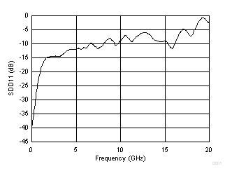
Figure 5-9 Input Return Loss Performance of the Downstream Ports
GUID-C0072D02-F404-45BF-8D91-C4ADAF4C549C-low.gif
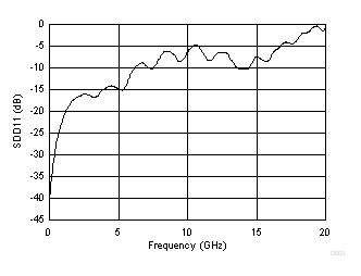
Figure 5-11 Input Return Loss Performance of the Upstream Ports
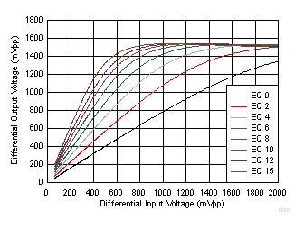
GUID-76F52931-56FB-4011-A6D1-7C88408C6FBF-low.gif
5 GHz
Figure 5-13 Downstream-to-Upstream Linearity Performance at 5 GHz
GUID-7DAA6F99-BEF0-473E-9F49-8B85AE6E0FA9-low.gif
100 MHz
Figure 5-15 Downstream-to-Upstream Linearity Performance at 100 MHz
GUID-51B184B4-B590-419B-8012-72AE04EF4C5D-low.gif
4.05 GHz
Figure 5-17 Upstream-to-Downstream Linearity Performance at 4.05 GHz
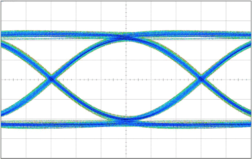
GUID-6C2FE5F5-9133-4EA2-9509-3AC4F10D0006-low.gif
Source: Data Rate: 10 Gbps; Data Pattern: PRBS7; Swing: 1 Vpp
Channel: Upstream-to-Downstream, 12 in 6 mil Input PCB Channel
Settings: EQ Setting: TBD; DC Gain Setting: 0 dB; Linear Range Setting: 1100 mVpp
Figure 5-19 Output Eye-Pattern Performance at 10 Gbps
GUID-F8EFBBFA-B162-441B-803D-15B574D704AF-low.gif
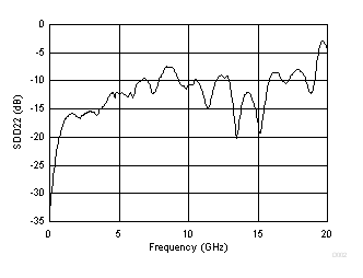
Figure 5-10 Output Return Loss Performance of the Downstream Ports
GUID-D9905C59-AACD-47E3-9427-2E7B5430D483-low.gif
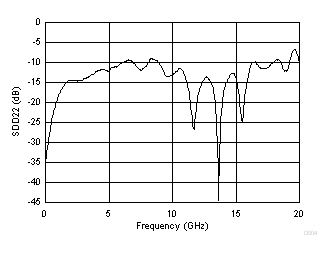
Figure 5-12 Output Return Loss Performance of the Upstream Ports
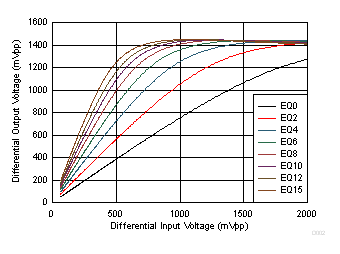
GUID-97F3F5D2-0D6C-4E16-911E-E8DE9FCDF9CB-low.gif
4.05 GHz
Figure 5-14 Downstream-to-Upstream Linearity Performance at 4.05 GHz
GUID-5F508D40-A6CB-4351-85E3-2DB9618D2E08-low.gif
5 GHz
Figure 5-16 Upstream-to-Downstream Linearity Performance at 5 GHz
GUID-45DE5278-2196-4108-8240-8D1595780DF3-low.gif
100 MHz
Figure 5-18 Upstream-to-Downstream Linearity Performance at 100 MHz
GUID-FC0FD984-0477-467F-B51A-CA949297AF67-low.gif
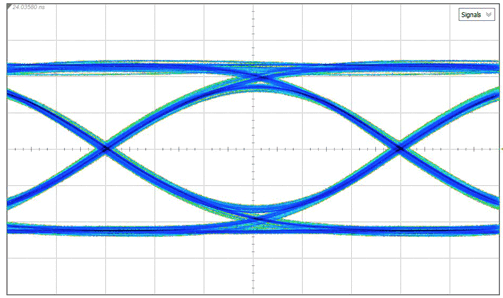
Source: Data Rate: 8.1 Gbps; Data Pattern: PRBS7; Swing: 1 Vpp
Channel: Upstream-to-Downstream, 12 in 6 mil Input PCB Channel
Settings: EQ Setting: 7; DC Gain Setting: 0 dB; Linear Range Setting: 1100 mVpp
Figure 5-20 Output Eye-Pattern Performance at 8.1 Gbps
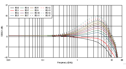
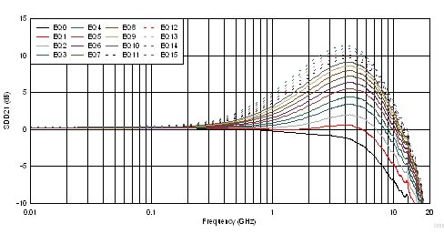
GUID-7F922070-371A-42A0-98E2-3F77A8F7B1B4-low.gif
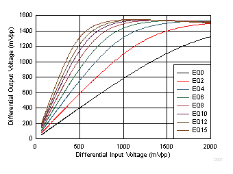
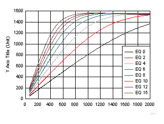
Figure 5-21 Upstream-to-Downstream EQ Settings Curves
GUID-1D3F31CB-A276-4274-83A0-32BB31743844-low.gif
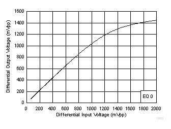
Figure 5-22 Downstream-to-Upstream EQ Settings Curves