SLLSEF7 March 2014 TUSB8020B-Q1
PRODUCTION DATA.
- 1 Features
- 2 Applications
- 3 Description
- 4 Revision History
- 5 Description (Continued)
- 6 Terminal Configuration and Functions
- 7 Specifications
-
8 Detailed Description
- 8.1 Overview
- 8.2 Functional Block Diagram
- 8.3 Feature Description
- 8.4 Device Functional Modes
- 8.5
Register Maps
- 8.5.1
Configuration Registers
- 8.5.1.1 ROM Signature Register
- 8.5.1.2 Vendor ID LSB Register
- 8.5.1.3 Vendor ID MSB Register
- 8.5.1.4 Product ID LSB Register
- 8.5.1.5 Product ID MSB Register
- 8.5.1.6 Device Configuration Register
- 8.5.1.7 Battery Charging Support Register
- 8.5.1.8 Device Removable Configuration Register
- 8.5.1.9 Port Used Configuration Register
- 8.5.1.10 PHY Custom Configuration Register
- 8.5.1.11 Device Configuration Register 2
- 8.5.1.12 UUID Registers
- 8.5.1.13 Language ID LSB Register
- 8.5.1.14 Language ID MSB Register
- 8.5.1.15 Serial Number String Length Register
- 8.5.1.16 Manufacturer String Length Register
- 8.5.1.17 Product String Length Register
- 8.5.1.18 Serial Number Registers
- 8.5.1.19 Manufacturer String Registers
- 8.5.1.20 Product String Registers
- 8.5.1.21 Additional Feature Configuration Register
- 8.5.1.22 Charging Port Control Register
- 8.5.1.23 Device Status and Command Register
- 8.5.1
Configuration Registers
- 9 Applications and Implementation
- 10Power Supply Recommendations
- 11Layout
- 12Device and Documentation Support
- 13Mechanical, Packaging, and Orderable Information
Package Options
Mechanical Data (Package|Pins)
- PHP|48
Thermal pad, mechanical data (Package|Pins)
- PHP|48
Orderable Information
9 Applications and Implementation
9.1 Application Information
The TUSB8020B-Q1 is a two-port USB 3.0 compliant hub. It provides simultaneous SuperSpeed USB and high-speed/full-speed connections on the upstream port and provides SuperSpeed USB, high-speed, full-speed, or low speed connections on the downstream port. The TUSB8020B-Q1 can be used in any application that needs additional USB compliant ports. For example, a specific notebook may only have two downstream USB ports. By using the TUSB8020B-Q1, the notebook can increase the downstream port count to three.
9.2 Typical Applications
A common application for the TUSB8020B-Q1 is as a self powered standalone USB hub product. The product is powered by an external 5V DC Power adapter. In this application, using a USB cable TUSB8020B-Q1’s upstream port is plugged into a USB Host controller. The downstream ports of the TUSB8020B-Q1 are exposed to users for connecting USB hard drives, camera, flash drive, and so forth.
 Figure 3. Discrete USB Hub Product
9.2.1 Design Requirements
Table 50. Input Parameters
| DESIGN PARAMETER | EXAMPLE VALUE |
|---|---|
| VDD Supply | 1.1V |
| VDD33 Supply | 3.3V |
| Upstream Port USB Support (SS, HS, FS) | SS, HS, FS |
| Downstream Port 1 USB Support (SS, HS, FS, LS) | SS, HS, FS, LS |
| Downstream Port 2 USB Support (SS, HS, FS, LS) | SS, HS, FS, LS |
| # of Removable Downstream Ports | 2 |
| # of Non-Removable Downstream Ports | 0 |
| Full Power Management of Downstream Ports | Yes. (FULLPWRMGMTZ = 0) |
| Individual Control of Downstream Port Power Switch | Yes. (GANGED = 0) |
| Power Switch Enable Polarity | Active High. (PWRCTL_POL = 0) |
| Battery Charge Support for Downstream Port 1 | Yes |
| Battery Charge Support for Downstream Port 2 | Yes |
| I2C EEPROM Support | No. |
| 24MHz Clock Source | Crystal |
9.2.2 Detailed Design Procedure
9.2.2.1 Upstream Port Implementation
The upstream of the TUSB8020B-Q1 is connected to a USB3 Type B connector. This particular example has GANGED terminal and FULLPWRMGMTZ terminal pulled low which results in individual power support each downstream port. The VBUS signal from the USB3 Type B connector is feed through a voltage divider. The purpose of the voltage divider is to make sure the level meets USB_VBUS input requirements.
 Figure 4. Upstream Port Implementation
9.2.2.2 Downstream Port 1 Implementation
The downstream port 1 of the TUSB8020B-Q1 is connected to a USB3 Type A connector. With BATEN1 terminal pulled up, Battery Charge support is enabled for Port 1. If Battery Charge support is not needed, then pull-up resistor on BATEN1 should be uninstalled. The PWRCTL_POL is pulled down which will result in active high power enable (PWRCTL1 and PWRCTL2) for a USB VBUS power switch.
 Figure 5. Downstream Port 1 Implementation
9.2.2.3 Downstream Port 2 Implementation
The downstream port 2 of the TUSB8020B-Q1 is connected to a USB3 Type A connector. With BATEN2 terminal pulled up, Battery Charge support is enabled for Port 2. If Battery Charge support is not needed, then pull-up resistor on BATEN2 should be uninstalled.
 Figure 6. Downstream Port 2 Implementation
9.2.2.4 VBUS Power Switch Implementation
This particular example uses the Texas Instruments TPS2561 dual channel precision adjustable current-limited power switch. For details on this power switch or other power switches available from Texas Instruments, please refer to the Texas Instruments website.
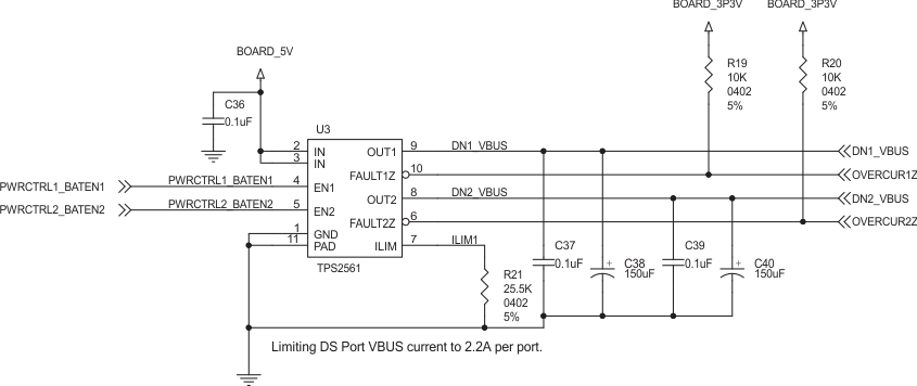 Figure 7. Power Switch Implementation
9.2.2.5 Clock, Reset, and Misc
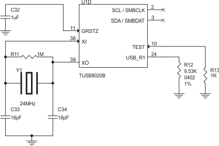 Figure 8. Clock, Reset, and Misc
9.2.2.6 Power Implementation
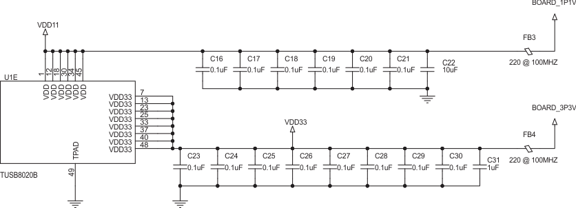 Figure 9. Power Implementation
9.2.3 Application Curves
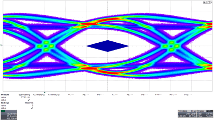 Figure 10. SuperSpeed TX Eye for Downstream Port 1
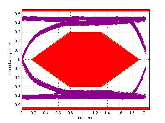 Figure 12. : HighSpeed TX Eye for Downstream Port 1
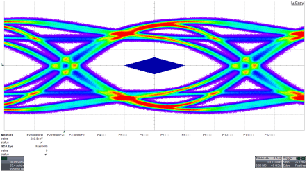 Figure 11. : SuperSpeed TX Eye for Downstream Port 2
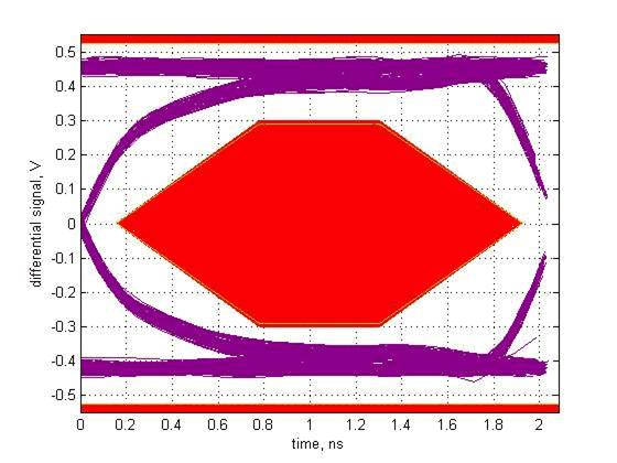 Figure 13. HighSpeed TX Eye for Downstream Port 2