SLLSEF7 March 2014 TUSB8020B-Q1
PRODUCTION DATA.
- 1 Features
- 2 Applications
- 3 Description
- 4 Revision History
- 5 Description (Continued)
- 6 Terminal Configuration and Functions
- 7 Specifications
-
8 Detailed Description
- 8.1 Overview
- 8.2 Functional Block Diagram
- 8.3 Feature Description
- 8.4 Device Functional Modes
- 8.5
Register Maps
- 8.5.1
Configuration Registers
- 8.5.1.1 ROM Signature Register
- 8.5.1.2 Vendor ID LSB Register
- 8.5.1.3 Vendor ID MSB Register
- 8.5.1.4 Product ID LSB Register
- 8.5.1.5 Product ID MSB Register
- 8.5.1.6 Device Configuration Register
- 8.5.1.7 Battery Charging Support Register
- 8.5.1.8 Device Removable Configuration Register
- 8.5.1.9 Port Used Configuration Register
- 8.5.1.10 PHY Custom Configuration Register
- 8.5.1.11 Device Configuration Register 2
- 8.5.1.12 UUID Registers
- 8.5.1.13 Language ID LSB Register
- 8.5.1.14 Language ID MSB Register
- 8.5.1.15 Serial Number String Length Register
- 8.5.1.16 Manufacturer String Length Register
- 8.5.1.17 Product String Length Register
- 8.5.1.18 Serial Number Registers
- 8.5.1.19 Manufacturer String Registers
- 8.5.1.20 Product String Registers
- 8.5.1.21 Additional Feature Configuration Register
- 8.5.1.22 Charging Port Control Register
- 8.5.1.23 Device Status and Command Register
- 8.5.1
Configuration Registers
- 9 Applications and Implementation
- 10Power Supply Recommendations
- 11Layout
- 12Device and Documentation Support
- 13Mechanical, Packaging, and Orderable Information
Package Options
Mechanical Data (Package|Pins)
- PHP|48
Thermal pad, mechanical data (Package|Pins)
- PHP|48
Orderable Information
6 Terminal Configuration and Functions
PHP Package
(Top View)
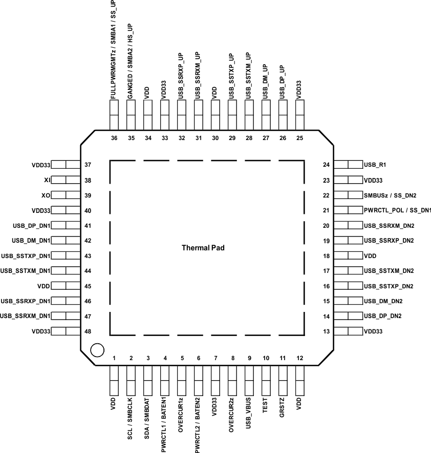
Terminal Functions
| TERMINAL | TYPE(1) | DESCRIPTION | ||||||||
|---|---|---|---|---|---|---|---|---|---|---|
| NAME | TERMINAL NO. |
|||||||||
| Clock and Reset Signals | ||||||||||
| GRSTz | 11 | I PU |
Global power reset. This reset brings all of the TUSB8020B-Q1 internal registers to their default states. When GRSTz is asserted, the device is completely nonfunctional. | |||||||
| XI | 38 | I | Crystal input. This terminal is the crystal input for the internal oscillator. The input may alternately be driven by the output of an external oscillator. When using a crystal a 1-MΩ feedback resistor is required between XI and XO. | |||||||
| XO | 39 | O | Crystal output. This terminal is the crystal output for the internal oscillator. If XI is driven by an external oscillator this pin may be left unconnected. When using a crystal a 1-MΩ feedback resistor is required between XI and XO. | |||||||
| USB Upstream Signals | ||||||||||
| USB_SSTXP_UP | 29 | O | USB SuperSpeed transmitter differential pair (positive) | |||||||
| USB_SSTXM_UP | 28 | O | USB SuperSpeed transmitter differential pair (negative) | |||||||
| USB_SSRXP_UP | 32 | I | USB SuperSpeed receiver differential pair (positive) | |||||||
| USB_SSRXM_UP | 31 | I | USB SuperSpeed receiver differential pair (negative) | |||||||
| USB_DP_UP | 26 | I/O | USB High-speed differential transceiver (positive) | |||||||
| USB_DM_UP | 27 | I/O | USB High-speed differential transceiver (negative) | |||||||
| USB_R1 | 24 | I | Precision resistor reference. A 9.53-kΩ ±1% resistor should be connected between USB_R1 and GND. | |||||||
| USB_VBUS | 9 | I | USB upstream port power monitor. The VBUS detection requires a voltage divider. The signal USB_VBUS must be connected to VBUS through a 90.9-KΩ ±1% resistor, and to ground through a 10-kΩ ±1% resistor from the signal to ground. |
|||||||
| USB Downstream Signals | ||||||||||
| USB_SSTXP_DN1 | 43 | O | USB SuperSpeed transmitter differential pair (positive) Downstream Port 1. | |||||||
| USB_SSTXM_DN1 | 44 | O | USB SuperSpeed transmitter differential pair (negative) Downstream Port 1. | |||||||
| USB_SSRXP_DN1 | 46 | I | USB SuperSpeed receiver differential pair (positive) Downstream Port 1. | |||||||
| USB_SSRXM_DN1 | 47 | I | USB SuperSpeed receiver differential pair (negative) Downstream Port 1. | |||||||
| USB_DP_DN1 | 41 | I/O | USB High-speed differential transceiver (positive) Downstream Port 1. | |||||||
| USB_DM_DN1 | 42 | I/O | USB High-speed differential transceiver (negative) Downstream Port 1. | |||||||
| PWRCTL1/BATEN1 | 4 | I/O, PD | USB Port 1 Power On Control for Downstream Power/Battery Charging Enable. The terminal is used for control of the downstream power switch for Port 1. | |||||||
| In addition, the value of the terminal is sampled at the de-assertion of reset to determine the value of the battery charging support for Port 1 as indicated in the Battery Charging Support register. | ||||||||||
| 0 = Battery charging not supported | ||||||||||
| 1 = Battery charging supported | ||||||||||
| OVERCUR1z | 5 | I, PU | USB DS Port 1 Over-Current Detection input. This terminal is used to connect the over current output of the downstream port power switch for Port 1. | |||||||
| 0 = An over current event has occurred | ||||||||||
| 1 = An over current event has not occurred | ||||||||||
| If power management is enabled, the external circuitry needed should be determined by the power switch. In ganged mode either OVERCUR1z or OVERCUR2z can be used. In ganged mode the overcurrent will be reported as a hub event instead of a port event. | ||||||||||
| USB_SSTXP_DN2 | 16 | O | USB SuperSpeed transmitter differential pair (positive) Downstream Port 2. | |||||||
| USB_SSTXM_DN2 | 17 | O | USB SuperSpeed transmitter differential pair (negative) Downstream Port 2. | |||||||
| USB_SSRXP_DN2 | 19 | I | USB SuperSpeed receiver differential pair (positive) Downstream Port 2. | |||||||
| USB_SSRXM_DN2 | 20 | I | USB SuperSpeed receiver differential pair (negative) Downstream Port 2. | |||||||
| USB_DP_DN2 | 14 | I/O | USB High-speed differential transceiver (positive) Downstream Port 2. | |||||||
| USB_DM_DN2 | 15 | I/O | USB High-speed differential transceiver (negative) Downstream Port 2. | |||||||
| PWRCTL2/BATEN2 | 6 | I/O, PD | Power On Control /Battery Charging Enable for Downstream Port 2. This terminal is used for control of the downstream power switch for Port 2. | |||||||
| In addition, the value of the terminal is sampled at the de-assertion of reset to determine the value of the battery charging support for Port 2 as indicated in the Battery Charging Support register. | ||||||||||
| 0 = Battery charging not supported | ||||||||||
| 1 = Battery charging supported | ||||||||||
| OVERCUR2z | 8 | I, PU | Over-Current Detection for Downstream Port 2. This terminal is used to connect the over current output of the downstream port power switch for Port 2. | |||||||
| 0 = An over current event has occurred | ||||||||||
| 1 = An over current event has not occurred | ||||||||||
| If power management is enabled, the external circuitry needed should be determined by the power switch. In ganged mode either OVERCUR1z or OVERCUR2z can be used. In ganged mode the overcurrent will be reported as a hub event instead of a port event. | ||||||||||
| I2C/SMBUS Signals | ||||||||||
| SCL/SMBCLK | 2 | I/O, PD | I2C clock/SMBus clock. Function of terminal depends on the setting of the SMBUSz input. | |||||||
| When SMBUSz = 1, this terminal acts as the serial clock interface for an I2C EEPROM. | ||||||||||
| When SMBUSz = 0, this terminal acts as the serial clock interface for an SMBus host. | ||||||||||
| This pin must be pulled up to use the OTP ROM. | ||||||||||
| Can be left unconnected if external interface not implemented. | ||||||||||
| SDA/SMBDAT | 3 | I/O, PD | I2C data/SMBus data. Function of terminal depends on the setting of the SMBUSz input. | |||||||
| When SMBUSz = 1, this terminal acts as the serial data interface for an I2C EEPROM. | ||||||||||
| When SMBUSz = 0, this terminal acts as the serial data interface for an SMBus host. | ||||||||||
| This pin must be pulled up to use the OTP ROM. | ||||||||||
| Can be left unconnected if external interface not implemented. | ||||||||||
| Test and Miscellaneous Signals | ||||||||||
| SMBUSz/SS_DN2 | 22 | I, PU | SMBUS mode / SuperSpeed USB Status for Downstream Port 2 | |||||||
| The value of the terminal is sampled at the de-assertion of reset to enable I2C or SMBus mode. | ||||||||||
| 0 = SMBus Mode Selected | ||||||||||
| 1 = I2C mode selected | ||||||||||
| After reset, this signal indicates the SuperSpeed USB connection status of downstream port 2. A value of 1 indicates the connection is SuperSpeed USB. | ||||||||||
| PWRCTL_POL/SS_DN1 | 21 | I/O, PD | Power Control Polarity / SuperSpeed USB Status for Downstream Port 1. | |||||||
| The value of the terminal is sampled at the de-assertion of reset to set the polarity of PWRCTL[2:1]. | ||||||||||
| 0 = PWRCTL polarity is active high. | ||||||||||
| 1 = PWRCTL polarity is active loiw. | ||||||||||
| After reset, this signal indicates the SuperSpeed USB connection status of downstream port 1. A value of 1 indicates the connection is SuperSpeed USB. | ||||||||||
| GANGED/SMBA2/ HS_UP |
35 | I, PU | Ganged operation enable/SMBus Address bit 2/ High-Speed Status for Upstream Port | |||||||
| The value of the terminal is sampled at the de-assertion of reset to set the power switch and over current detection mode as follows: | ||||||||||
| 0 = Individual power control supported when power switching is enabled. | ||||||||||
| 1 = Power control gangs supported when power switching is enabled. | ||||||||||
| When SMBus mode is enabled using SMBUSz, this terminal sets the value of the SMBus slave address bit 2. SMBus slave address bits 2 and 3 are always 1 for the TUSB8020B-Q1. | ||||||||||
| After reset, this signal indicates the High-speed USB connection status of the upstream port. A value of 1 indicates the upstream port is connected to a High-speed USB capable port. | ||||||||||
| FULLPWRMGMTz/ SMBA1/SS_UP |
36 | I, PU | Full power management enable/ SMBus Address bit 1/ Super-Speed USB Status for Upstream port | |||||||
| The value of the terminal is sampled at the de-assertion of reset to set the power switch control follows: | ||||||||||
| 0 = Power switching supported | ||||||||||
| 1 = Power switching not supported | ||||||||||
| Full power management is the ability to control power to the downstream ports of the TUSB8020B-Q1 using PWRCTL[2:1]/BATEN[2:1]. | ||||||||||
| When SMBus mode is enabled using SMBUSz, this terminal sets the value of the SMBus slave address bit 1. SMBus slave address bit 3 is always 1 for the TUSB8020B-Q1. | ||||||||||
| Can be left unconnected if full power management and SMBus are not implemented. | ||||||||||
| After reset, this signal indicates the SuperSpeed USB connection status of the upstream port. A value of 1 indicates the upstream port is connected to a SuperSpeed USB capable port. | ||||||||||
| TEST | 10 | I, PD | TEST mode enable. When this terminal is asserted high at reset enables test mode. This terminal is reserved for factory use. It is recommended to pull-down this terminal to ground. | |||||||
| Power and Ground Signals | ||||||||||
| VDD | 1, 12, 18, 30, 34, 45 | PWR | 1.1-V power rail | |||||||
| VDD33 | 7, 13, 23, 25, 33, 37, 40, 48 | PWR | 3.3-V power rail | |||||||
| GND | PAD | - | Ground | |||||||
(1) I = input, O = output, I/O = input/output, PU = internal pullup resistor, PD = internal pulldown resistor, and PWR = power signal