SLLSEF7 March 2014 TUSB8020B-Q1
PRODUCTION DATA.
- 1 Features
- 2 Applications
- 3 Description
- 4 Revision History
- 5 Description (Continued)
- 6 Terminal Configuration and Functions
- 7 Specifications
-
8 Detailed Description
- 8.1 Overview
- 8.2 Functional Block Diagram
- 8.3 Feature Description
- 8.4 Device Functional Modes
- 8.5
Register Maps
- 8.5.1
Configuration Registers
- 8.5.1.1 ROM Signature Register
- 8.5.1.2 Vendor ID LSB Register
- 8.5.1.3 Vendor ID MSB Register
- 8.5.1.4 Product ID LSB Register
- 8.5.1.5 Product ID MSB Register
- 8.5.1.6 Device Configuration Register
- 8.5.1.7 Battery Charging Support Register
- 8.5.1.8 Device Removable Configuration Register
- 8.5.1.9 Port Used Configuration Register
- 8.5.1.10 PHY Custom Configuration Register
- 8.5.1.11 Device Configuration Register 2
- 8.5.1.12 UUID Registers
- 8.5.1.13 Language ID LSB Register
- 8.5.1.14 Language ID MSB Register
- 8.5.1.15 Serial Number String Length Register
- 8.5.1.16 Manufacturer String Length Register
- 8.5.1.17 Product String Length Register
- 8.5.1.18 Serial Number Registers
- 8.5.1.19 Manufacturer String Registers
- 8.5.1.20 Product String Registers
- 8.5.1.21 Additional Feature Configuration Register
- 8.5.1.22 Charging Port Control Register
- 8.5.1.23 Device Status and Command Register
- 8.5.1
Configuration Registers
- 9 Applications and Implementation
- 10Power Supply Recommendations
- 11Layout
- 12Device and Documentation Support
- 13Mechanical, Packaging, and Orderable Information
Package Options
Mechanical Data (Package|Pins)
- PHP|48
Thermal pad, mechanical data (Package|Pins)
- PHP|48
Orderable Information
7 Specifications
7.1 Absolute Maximum Ratings
over operating free-air temperature range (unless otherwise noted)| VALUE | UNIT | ||
|---|---|---|---|
| VDD | Steady-state supply voltage | –0.3 to 1.4 | V |
| VDD33 | Steady-state supply voltage | –0.3 to 3.8 | V |
7.2 Handling Ratings
| MIN | MAX | UNIT | ||
|---|---|---|---|---|
| Tstg | Storage temperature range | –65 | 150 | °C |
| VESD | Human-Body Model (HBM) AEC-Q100 Classification Level H2 | 2000 | V | |
| Charged-Device Model (CDM) AEQ-Q100 Classification Level C4B for corner pins | 750 | |||
| Charged-Device Model (CDM) AEQ-Q100 Classification Level C4B for non-corner pins | 500 |
7.3 Recommended Operating Conditions
over operating free-air temperature range (unless otherwise noted)| MIN | NOM | MAX | UNIT | |||
|---|---|---|---|---|---|---|
| VDD(1) | 1.1 supply voltage | 0.99 | 1.1 | 1.26 | V | |
| VDD33 | 3.3 supply voltage | 3 | 3.3 | 3.6 | V | |
| USB_VBUS | Voltage at USB_VBUS PAD | 0 | 1.155 | V | ||
| TA | Operating free-air temperature range | -40 | 25 | 85 | °C | |
| TJ | Operating junction temperature range | -40 | 25 | 105 | °C | |
(1) A 1.05-V, 1.1-V, or 1.2-V supply may be used as long as minimum and maximum supply conditions are met.
7.4 Thermal Information
| THERMAL METRIC(1) | TUSB8020B-Q1 | UNIT | |
|---|---|---|---|
| PHP | |||
| 48 PIN | |||
| RθJA | Junction-to-ambient thermal resistance(2) | 31.8 | °C/W |
| RθJCtop | Junction-to-case (top) thermal resistance(3) | 16.1 | |
| RθJB | Junction-to-board thermal resistance(4) | 13 | |
| ψJT | Junction-to-top characterization parameter(5) | 0.5 | |
| ψJB | Junction-to-board characterization parameter(6) | 12.9 | |
| RθJCbot | Junction-to-case (bottom) thermal resistance(7) | 0.9 | |
(1) For more information about traditional and new thermal metrics, see the IC Package Thermal Metrics application report, SPRA953.
(2) The junction-to-ambient thermal resistance under natural convection is obtained in a simulation on a JEDEC-standard, high-K board, as specified in JESD51-7, in an environment described in JESD51-2a.
(3) The junction-to-case (top) thermal resistance is obtained by simulating a cold plate test on the package top. No specific JEDEC-standard test exists, but a close description can be found in the ANSI SEMI standard G30-88.
(4) The junction-to-board thermal resistance is obtained by simulating in an environment with a ring cold plate fixture to control the PCB temperature, as described in JESD51-8.
(5) The junction-to-top characterization parameter, ψJT, estimates the junction temperature of a device in a real system and is extracted from the simulation data for obtaining θJA, using a procedure described in JESD51-2a (sections 6 and 7).
(6) The junction-to-board characterization parameter, ψJB, estimates the junction temperature of a device in a real system and is extracted from the simulation data for obtaining θJA , using a procedure described in JESD51-2a (sections 6 and 7).
(7) The junction-to-case (bottom) thermal resistance is obtained by simulating a cold plate test on the exposed (power) pad. No specific JEDEC standard test exists, but a close description can be found in the ANSI SEMI standard G30-88.
7.5 3.3-V I/O Electrical Characteristics
over operating free-air temperature range (unless otherwise noted)| PARAMETER | OPERATION | TEST CONDITIONS | MIN | MAX | UNIT | |
|---|---|---|---|---|---|---|
| VIH | High-level input voltage(1) | VDD33 | 2 | VDD33 | V | |
| VIL | Low-level input voltage(1) | VDD33 | 0 | 0.8 | V | |
| VI | Input voltage | 0 | VDD33 | V | ||
| VO | Output voltage(2) | 0 | VDD33 | V | ||
| tt | Input transition time (trise and tfall) | 0 | 25 | ns | ||
| Vhys | Input hysteresis(3) | 0.13 x VDD33 | V | |||
| VOH | High-level output voltage | VDD33 | IOH = -4 mA | 2.4 | V | |
| VOL | Low-level output voltage | VDD33 | IOL = 4 mA | 0.4 | V | |
| IOZ | High-impedance, output current(2) | VDD33 | VI = 0 to VDD33 | ±20 | µA | |
| IOZP | High-impedance, output current with internal pullup or pulldown resistor(4) | VDD33 | VI = 0 to VDD33 | ±225 | µA | |
| II | Input current(5) | VDD33 | VI = 0 to VDD33 | ±15 | µA | |
(1) Applies to external inputs and bidirectional buffers.
(2) Applies to external outputs and bidirectional buffers.
(3) Applies to GRSTz.
(4) Applies to pins with internal pullups/pulldowns.
(5) Applies to external input buffers.
7.6 Power-Up Timing Requirements
| MIN | TYP | MAX | UNIT | ||
|---|---|---|---|---|---|
| Td1 | VDD33 stable before VDD stable. There is no timing relationship between VDD33 and VDD | 0 | ms | ||
| Td2 | VDD and VDD33 stable before de-assertion of GRSTZ. | 3 | ms | ||
| Tsu_io | Setup for MISC inputs sampled at the de-assertion of GRSTZ(1) | 0.1 | µs | ||
| Thd_io | Hold for MISC inputs sampled at the de-assertion of GRSTZ.(1) | 0.1 | µs | ||
| TVDD33_RAMP | VDD33 supply ramp requirements | 0.2 | 100 | ms | |
| TVDD_RAMP | VDD supply ramp requirements | 0.2 | 100 | ms | |
(1) Misc pins sampled at de-assertion of GRSTZ: FULLPWRMGMTz, GANGED, PWRCTL_POL, SMBUSz, BATEN1, and BATEN2
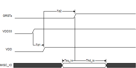 Figure 1. Power-Up Timing Requirements
7.7 Hub Input Supply Current
Typical values measured at TA = 25°C| PARAMETER | VDD33 | VDD11 | UNIT | |
|---|---|---|---|---|
| 3.3 V | 1.1 V | |||
| LOW POWER MODES | ||||
| Power On (after Reset) | 5 | 39 | mA | |
| Disconnect from Host | 5 | 39 | mA | |
| Suspend (USB2 Host) | 5 | 39 | mA | |
| Suspend (USB3 Host) | 6 | 40 | mA | |
| ACTIVE MODES (US state / DS State) | ||||
| 3.0 host / 1 SS Device and Hub in U1 | 50 | 218 | mA | |
| 3.0 host / 1 SS Device and Hub in U0 | 50 | 342 | mA | |
| 3.0 host / 2 SS Devices and Hub in U1 | 50 | 284 | mA | |
| 3.0 host / 2 SS Devices and Hub in U0 | 50 | 456 | mA | |
| 3.0 host / 1 SS and 1 HS Device in U1 | 92 | 242 | mA | |
| 3.0 host / 1 SS and 1 HS Device in U0 | 93 | 364 | mA | |
| 2.0 host / 1 HS Device active | 48 | 71 | mA | |
| 2.0 host / 2 HS Devices active | 60 | 80 | mA | |