SLUSCX6B February 2018 – February 2024 UCC21222
PRODUCTION DATA
- 1
- 1 Features
- 2 Applications
- 3 Description
- 4 Pin Configuration and Functions
-
5 Specifications
- 5.1 Absolute Maximum Ratings
- 5.2 ESD Ratings
- 5.3 Recommended Operating Conditions
- 5.4 Thermal Information
- 5.5 Power Ratings
- 5.6 Insulation Specifications
- 5.7 Safety-Related Certifications
- 5.8 Safety-Limiting Values
- 5.9 Electrical Characteristics
- 5.10 Switching Characteristics
- 5.11 Thermal Derating Curves
- 5.12 Typical Characteristics
- 6 Parameter Measurement Information
- 7 Detailed Description
-
8 Application and Implementation
- 8.1 Application Information
- 8.2
Typical Application
- 8.2.1 Design Requirements
- 8.2.2
Detailed Design Procedure
- 8.2.2.1 Custom Design With WEBENCH® Tools
- 8.2.2.2 Designing INA/INB Input Filter
- 8.2.2.3 Select Dead Time Resistor and Capacitor
- 8.2.2.4 Select External Bootstrap Diode and its Series Resistor
- 8.2.2.5 Gate Driver Output Resistor
- 8.2.2.6 Estimating Gate Driver Power Loss
- 8.2.2.7 Estimating Junction Temperature
- 8.2.2.8 Selecting VCCI, VDDA/B Capacitor
- 8.2.2.9 Application Circuits with Output Stage Negative Bias
- 8.2.3 Application Curves
- 9 Power Supply Recommendations
- 10Layout
- 11Device and Documentation Support
- 12Revision History
- 13Mechanical, Packaging, and Orderable Information
Package Options
Mechanical Data (Package|Pins)
- D|16
Thermal pad, mechanical data (Package|Pins)
Orderable Information
3 Description
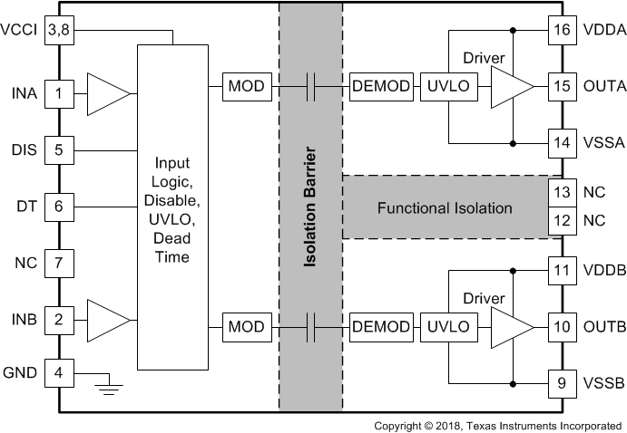
The UCC21222 device is an isolated dual channel gate driver with programmable dead time. It is designed with 4A peak-source and 6A peak-sink current to drive power MOSFET, IGBT, and GaN transistors.
The device can be configured as two low-side drivers, two high-side drivers, or a half-bridge driver. A 5ns delay matching performance allows two outputs to be paralleled, doubling the drive strength for heavy load conditions without risk of internal shoot-through.
The input side is isolated from the two output drivers by a 3.0kVRMS isolation barrier, with a minimum of 100V/ns common-mode transient immunity (CMTI).
Resistor programmable dead time gives the capability to adjust dead time for system constraints to improve efficiency and prevent output overlap. Other protection features include a disable feature to shut down both outputs simultaneously when DIS is set high, an integrated deglitch filter that rejects input transients shorter than 5ns, and negative voltage handling for up to –2V spikes for 200ns on input and output pins. All supplies have UVLO protection.
| PART NUMBER(1) | PACKAGE | BODY SIZE (NOM) |
|---|---|---|
| UCC21222 | D (SOIC 16) | 9.9mm × 3.91mm |
 Functional Block Diagram