SLUSBL6 February 2015 UCC24650
PRODUCTION DATA.
- 1 Features
- 2 Applications
- 3 Description
- 4 Revision History
- 5 Pin Configuration and Functions
- 6 Specifications
- 7 Detailed Description
- 8 Application and Implementation
- 9 Power Supply Recommendations
- 10Layout
- 11Device and Documentation Support
- 12Mechanical, Packaging, and Orderable Information
Package Options
Mechanical Data (Package|Pins)
- DBV|5
Thermal pad, mechanical data (Package|Pins)
Orderable Information
8 Application and Implementation
NOTE
Information in the following applications sections is not part of the TI component specification, and TI does not warrant its accuracy or completeness. TI’s customers are responsible for determining suitability of components for their purposes. Customers should validate and test their design implementation to confirm system functionality.
8.1 Application Information
The UCC24650 Wake-Up monitor is intended to be used with the UCC28730 PSR controller in off-line isolated DCM flyback converters. The UCC24650 signals the UCC28730 that the output voltage has drooped. This allows the PSR controller to react to a load increase even while operating at extremely-low switching frequencies. This pair of devices also operates at very-low bias currents to facilitate the achievement of <5 mW of input power consumption during the no-load operating condition.
8.2 Typical Application
A typical application for the UCC24650 uses the compatible UCC28730 PSR controller to regulate an isolated low-voltage DC output from a high-voltage AC source. As shown in Figure 19 and Figure 20, the output rectification can use a ground-referenced diode, or a ground-referenced synchronous rectifier, respectively.
NOTE
These figures are simplified to illustrate the basic application of the UCC24650 and do not show all of the components and networks needed for an actual converter design.
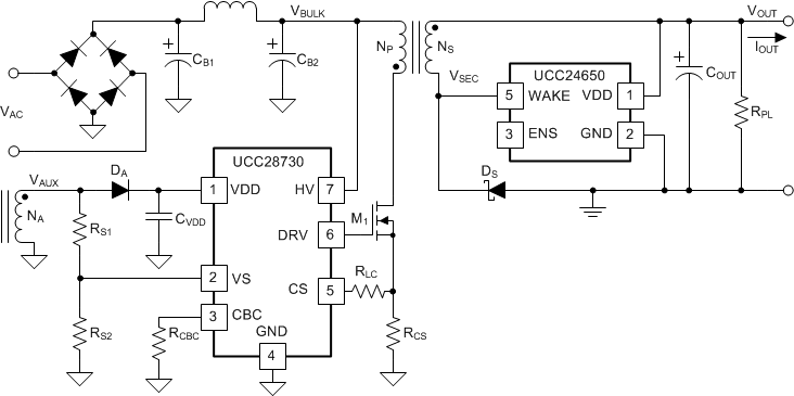 Figure 19. Simplified Application With Ground-Referenced Diode
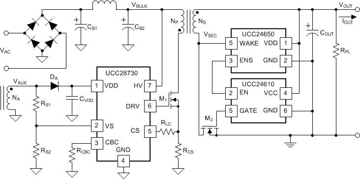 Figure 20. Simplified Application With Ground-Referenced Synchronous Rectifier
8.2.1 Design Requirements
Among the usual converter design requirements, the UCC24650 is especially suited to aid in achieving fast load-transient response and extremely-low input standby power. In many cases, the designer can achieve <5 mW of standby power, often referred to as Zero-Power.
8.2.2 Detailed Design Procedure
There is little design work required to use this device. Most calculations involve verification that the external conditions remain within the device’s various parameter operating limits.
Major design items to cover are:
- Ensure sufficient margin between lowest droop expected and the device UVLO threshold. The UVLO threshold is approximately 3.75 V and the compatible PSR controller usually requires some short time to respond to the WAKE signal and arrest the load-step droop. The minimum regulation voltage compatible with the use of this device must account for the anticipated droop plus any additional droop due to threshold reset and PSR response limitations.
- Ensure the maximum switching period tSW(max) is not exceeded, or the droop threshold may drift lower or higher and become inaccurate.
- Ensure the system-level VOUT overshoot remains below the device VDD absolute maximum rating.
- Ensure the system-level VSEC spike overshoot remains below the device WAKE absolute maximum rating.
- Ensure the system switched-node impedance allows sufficient signal amplitude so that the PSR controller is able to detect it. If necessary, a PNP emitter-follower buffer may be inserted between the WAKE pin and the secondary winding to boost the wake-up signal current level.
- Determine WAKE series resistance to limit current out of terminal, if necessary.
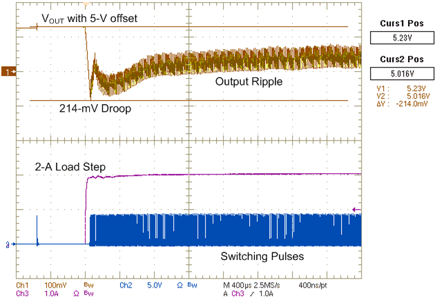
8.2.3 Application Curves
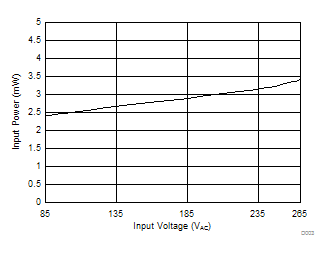
The following figures indicate the transient response of a 5-V, 10-W flyback converter which receives a pulsed step-load of 2 A while operating in the no-load standby condition. Figure 24 indicates the no-load standby input power consumption achieved by this converter over the full AC input range. Zero-Power operation is achieved while retaining fast transient response to a full load step.
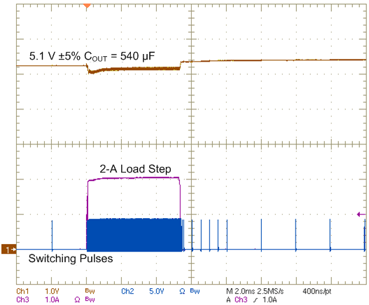 Figure 21. 2-A Load Step During Standby Operation
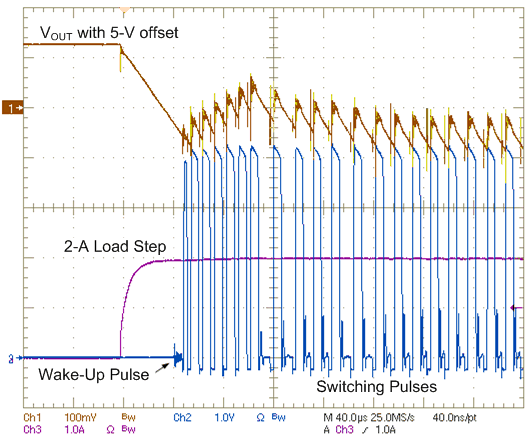 Figure 23. Wake-Up Pulse Triggering Response from UCC28730 Primary-Side Controller