SLUSBL6 February 2015 UCC24650
PRODUCTION DATA.
- 1 Features
- 2 Applications
- 3 Description
- 4 Revision History
- 5 Pin Configuration and Functions
- 6 Specifications
- 7 Detailed Description
- 8 Application and Implementation
- 9 Power Supply Recommendations
- 10Layout
- 11Device and Documentation Support
- 12Mechanical, Packaging, and Orderable Information
Package Options
Mechanical Data (Package|Pins)
- DBV|5
Thermal pad, mechanical data (Package|Pins)
Orderable Information
10 Layout
10.1 Layout Guidelines
There are no critical layout requirements. TI recommends to use the usual industry good-practice layout guidelines and principles.
To increase the reliability and feasibility of the project, TI recommends adhering to the following guidelines for PCB layout:
- Connect the WAKE and GND signals close to the output rectifier pads to minimize the effect of high di/dt and stray inductance on the WAKE pin voltage at the beginning of the flyback demagnetization time. It is not so important to minimize the WAKE and GND sense track lengths, rather to minimize the inductance between the two sense points at the rectifier.
- If ENS is not used, connect it to the GND pin to prevent the ENS input voltage from going below GND due to possible system noise.
10.2 Layout Example
The partial layout example of Figure 25 demonstrates an effective component and track arrangement for low-noise operation on a single-layer PCB. Actual board layout must conform to the constraints on a specific design, so many variations are possible.
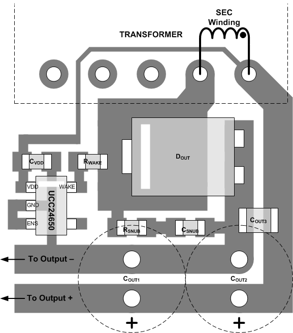 Figure 25. UCC24650 Partial Layout Example