SLUSBL6 February 2015 UCC24650
PRODUCTION DATA.
- 1 Features
- 2 Applications
- 3 Description
- 4 Revision History
- 5 Pin Configuration and Functions
- 6 Specifications
- 7 Detailed Description
- 8 Application and Implementation
- 9 Power Supply Recommendations
- 10Layout
- 11Device and Documentation Support
- 12Mechanical, Packaging, and Orderable Information
Package Options
Mechanical Data (Package|Pins)
- DBV|5
Thermal pad, mechanical data (Package|Pins)
Orderable Information
5 Pin Configuration and Functions
DBV Package
5-Pin SOT-23
Top View
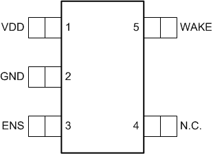
A. (N.C. = No connection internally)
Pin Functions
| PIN | I/O(1) | DESCRIPTION | |
|---|---|---|---|
| NAME | NO. | ||
| VDD | 1 | P | VDD is the bias supply input pin to the controller. This pin is continuously monitored to detect when the VDD voltage droops by approximately –3% of the previously sampled level. The VDD level is sampled and stored at the end of each power cycle generated by the PSR. The device is disabled when the VDD voltage is below the UVLO threshold. |
| GND | 2 | G | The ground pin is both the reference pin for the controller and the low-side return for the WAKE output. Take special care to return all AC decoupling capacitors as close as possible to this pin and avoid any common trace length with analog signal return paths. |
| ENS | 3 | O | Enable secondary circuit is an open-drain MOSFET output that enables a compatible synchronous rectifier (SR) controller or other secondary-side circuitry. ENS is open during normal operation and becomes low-impedance to GND when each switching period remains greater than tDISS (177 µs typical) for 63 consecutive cycles. ENS becomes high-impedance again when the switching period operates at less than tENS (57 µs typical) for 32 cumulative cycles. If the ENS function is not used, this terminal should be connected to GND. |
| N/C | 4 | — | The no-connection pin has no internal electrical connection. |
| WAKE | 5 | I/O | WAKE is a multi-function pin which connects to the transformer secondary winding, directly across the ground-referenced diode or rectifier. As an input, it monitors voltage pulses due to primary-side controller activity and triggers sampling of the VDD voltage at the end of each power cycle. When the WAKE voltage falls below 55 mV for >500 ns, the device becomes armed to deliver a power cycle detect (PCD) pulse internally. When the WAKE voltage subsequently rises above 55 mV, a PCD pulse is delivered to reset the oscillator, clock the PCD counter, and trigger a new sample of the VDD voltage. If the VDD voltage droops to 97% of the last sampled value, WAKE is driven as an output. As an output, it injects current into the transformer winding for 1 µs at a 33-kHz rate until a power cycle is detected. The maximum magnitude that this current may achieve is limited internally. |
(1) P = Power, G = Ground, I = Input, O = Output, I/O = Input/Output