SLUSAD7B April 2011 – July 2016 UCC25710
PRODUCTION DATA.
- 1 Features
- 2 Applications
- 3 Description
- 4 Revision History
- 5 Description (continued)
- 6 Pin Configuration and Functions
- 7 Specifications
- 8 Detailed Description
-
9 Application and Implementation
- 9.1 Application Information
- 9.2
Typical Application
- 9.2.1 Design Requirements
- 9.2.2
Detailed Design Procedure
- 9.2.2.1 Determining Transformer and Resonant Circuit Parameters
- 9.2.2.2 CS (Output Current Sense)
- 9.2.2.3 ICOMP (Current Amplifier Compensation)
- 9.2.2.4 SS (Soft Start)
- 9.2.2.5 FMAX (Maximum VCO Frequency)
- 9.2.2.6 FMIN (Minimum VCO Frequency)
- 9.2.2.7 GD1 and GD2 (Gate Drive 1 and 2)
- 9.2.2.8 LEDSW (LED Switch Drive)
- 9.2.2.9 DSR (Dimming Slew Rate)
- 9.2.2.10 DTY (Dimming Duty-Cycle Average)
- 9.2.2.11 DADJ (Dimming Duty-Cycle Adjust)
- 9.2.2.12 OV (Output Overvoltage)
- 9.2.2.13 UV (Output Undervoltage)
- 9.2.2.14 CL (Current Limit)
- 9.2.3 Application Curves
- 10Power Supply Recommendations
- 11Layout
- 12Device and Documentation Support
- 13Mechanical, Packaging, and Orderable Information
Package Options
Mechanical Data (Package|Pins)
- DW|20
Thermal pad, mechanical data (Package|Pins)
Orderable Information
9 Application and Implementation
NOTE
Information in the following applications sections is not part of the TI component specification, and TI does not warrant its accuracy or completeness. TI’s customers are responsible for determining suitability of components for their purposes. Customers should validate and test their design implementation to confirm system functionality.
9.1 Application Information
The UCC25710 offers a highly integrated solution for LLC control of LED lighting. To the part easier to use, TI has prepared an extensive set of materials to demonstrate the features of the device. The UCC25710 offers a highly integrated feature-set and excellent accuracy to control the LED current in highly efficient LLC type power supplies with dimming or without dimming requirements.
9.2 Typical Application
To take advantage of all the benefits integrated in this controller, the following procedure simplifies the setup to avoid unnecessary iterations in the design procedure. See Figure 24 setup for component names.
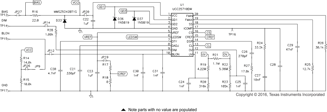 Figure 24. UCC25710 Controller Setup
9.2.1 Design Requirements
Table 1 lists the design parameters of this example.
Table 1. Design Parameters
| PARAMETER | MIN | TYP | MAX | UNIT | |
|---|---|---|---|---|---|
| INPUT CHARACTERISTICS | |||||
| VIN | Input voltage | 370 | 390 | 410 | V |
| IIN | Input current | 0.275 | A | ||
| OUTPUT1, OUTPUT2, OUTPUT3, OUTPUT 4 CHARACTERISTICS | |||||
| VLED1, VLED2, VLED3, VLED4 |
Output voltage set by LED load | 96 | 98 | 100 | V |
| ILED1, ILED2, ILED3, ILED4 |
Output current ripple | 0.0125 | AP-P | ||
| ILED1, ILED2, ILED3, ILED4 |
Output current | 0.245 | 0.25 | 0.255 | A |
| ILED1, ILED2, ILED3, ILED4 |
Line regulation | 0.245 | 0.25 | 0.255 | |
| ILED1, ILED2, ILED3, ILED4 |
Load regulation | 0.245 | 0.25 | 0.255 | |
| VOVP | Single output OVP | 136 | V | ||
| VUV | Single output undervoltage | 43 | |||
| Dimming range | 1% | 100% | |||
| Dimming frequency | 270 | 300 | 330 | Hz | |
| Current matching between strings (10% to 100% dimming) | –2% | 2% | |||
| Output power single output | 24.5 | W | |||
| Full output power | |||||
| SYSTEM CHARACTERISTICS | |||||
| FSW | 84 | 156 | kHz | ||
| η | 91% | 93% | |||
9.2.2 Detailed Design Procedure
9.2.2.1 Determining Transformer and Resonant Circuit Parameters
The muti-transformer architecture is similar to conventional LLC converter design with a few exceptions that are described in this section. Typical LLC voltage output converters are designed to operate nominally close to resonance and have the minimum switching frequency below resonance and maximum frequency above resonance. TI recommends operating above resonance at the nominal input voltage range of the converter to achieve good transient response during dimming and improved LED current matching. The transformer turns ratio equation shown is to target operation above resonance.
Use Equation 2 to calculate the turns ratio of the transformers in the multi-transformer architecture.

where
- N is the primary to secondary turns ratio
- NP is the primary turns
- NS is the secondary turns
- VIN is the input voltage to the LLC converter, typically the output of the PFC boost converter
- NT is the number of transformers
- VLED is the LED string voltage
Another important consideration for the multi-transformer LED driver is to set the total magnetizing inductance of the transformers as high as possible to minimize the primary magnetizing current and it’s effect on LED current matching. TI recommends targeting the total magnetizing inductance of the transformers to a value just low enough to achieve ZVS operation during nominal frequency operation. Equation 3 and Equation 4 determine the magnetizing inductance target. Reduce the calculated LM to accommodate LM and COSS tolerances.


where
- IMPk is the peak magnetizing current
- COSS is the MOSFET equivalent time related drain to source capacitance
- VIN is the nominal input voltage to the half bridge, normally the PFC output voltage
- FSW is the switching frequency at the regulation operating point
- LM is the magnetizing inductance of each transformer
- NT is the number of transformers with the primaries in series
To use standard LLC converter design process and available tools such as SLUC253 design calculator available on the TI website, the multiple transformers and reflected loads can be combined into one equivalent transformer and load as shown in Figure 25. Once Lr and Lm are determined based on a single transformer circuit, simply divide by the number of transformers for each transformer specification target.
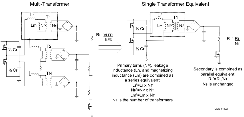 Figure 25. Multiple Transformers Combined With Reflected Loads
9.2.2.2 CS (Output Current Sense)
The CS pin is connected to the output current-sense resistor and is the feedback signal for the current amplifier. The regulation range is limited by the 0.5-V to 2.8-V internal current amplifier reference clamp. The LED current sense resistor value is determined by Equation 5.

where
- VCREF is voltage on CREF pin determined by divider from VREF ILEDTotal.
- ILEDTOTAL is the total LED string current during the DIM on time.
9.2.2.3 ICOMP (Current Amplifier Compensation)
Connect a capacitor or series resistor capacitor combination to ground to compensate the 510-µS GM current amplifier control loop. The current amplifier is designed to maintain the steady-state operating voltage point of the current amplifier during dimming operation. This is accomplished by switching on and off the GM current amplifier to the ICOMP pin with the same control signal that controls the LEDSW output. The GM amplifier is disconnected from the ICOMP pin during the DIM OFF-time, and connected during the DIM ON-time. This feature is compromised if there is a leakage path on the ICOMP pin, such as resistance to ground. The re-connection of the ICOMP pin to the current amplifier output is delayed by about 2.4 µs to allow time for the external LED switch to be turned on prior to allowing the ICOMP pin voltage to be driven.
The optimum ICOMP capacitor value is determined based on desired LED current and primary current response during dimming. Because the LLC converter has a highly nonlinear transfer function, a gain phase analyzer is recommended to optimize the component values on ICOMP. The recommended bandwidth target is from 800 Hz to 5 kHz. The trade-off of too low bandwidth is increased line frequency ripple on the LED string current. The trade-off of high bandwidth is voltage variation on ICOMP during the DSR rise time which can result in primary current peaking during the start of the DIM period, this may result in audible noise if excessive. Either an integrator (capacitor to ground) or type II compensation (capacitor in parallel with resistor and series capacitor) is recommended.
9.2.2.4 SS (Soft Start)
Connect a capacitor to ground to program the desired soft-start time. When VCC exceeds the VCCON threshold and BLON is high, a 2.5-µA current source charges the soft-start capacitor after a 10-ms delay. The voltage on SS dominates the VCO control voltage when lower than VICOMP or VDSR. The device is in a soft-start condition until VSS reaches the 4.2-V soft start over threshold. During the soft-start cycle DIM is disabled and the UV protection is disabled. The soft-start cycle is initiated by UVLO, BLON, OV fault clear, or UV fault clear after the soft-start cycle.

where
- TSS is the target SS time.
- VICOMP_REG is the ICOMP voltage at the regulation point, which can be derived based on LLC switching frequency.
9.2.2.5 FMAX (Maximum VCO Frequency)
Terminate FMAX to ground with a resistor to program the frequency delta from desired maximum to minimum operating frequency range. The recommended resistor value range is 4.22 kΩ to 53.6 kΩ. VICOMP which is the VCO control signal determines the voltage on FMAX; the programming resistor determines the voltage to current conversion ratio that programs the oscillator frequency at a given VICOMP voltage level. The device is designed to accommodate a maximum frequency of 350 kHz and a minimum frequency delta of 25 kHz. To provide controlled rise and fall time of the primary current during dimming, a maximum frequency of 2 to 3 times the nominal switching frequency is recommended as an initial value. The resistor value can be determined by Equation 7.

where
- FSW(Delta) = FSW(max)-FSW(min)
9.2.2.6 FMIN (Minimum VCO Frequency)
Terminate FMIN to ground with a resistor to program the desired minimum operating frequency. The recommended resistor range is 9.53 kΩ to 102 kΩ. The device is designed to accommodate a minimum frequency of 30 KHz. The resistor value can be determined by Equation 8.

Use Equation 9 to determine FSW for given VICOMP, RFMAX, and RFMIN values.

where
- FSW is in Hz, R is in Ω
- VICOMP is in V
9.2.2.7 GD1 and GD2 (Gate Drive 1 and 2)
Connect the primary of the gate-drive transformer to GD1 and GD2 through a small series resistance. The high-side driver resistance is 12 Ω and low-side driver resistance is 4 Ω typical. The drivers are limited to 25-mA RMS maximum current, so there is a magnetizing current limitation of the gate-drive transformer shown in the Equation 10. If the magnetizing current exceeds 25 mA with the specified gate-drive transformer and nominal operating frequency, a simple NPN-PNP buffer on GD1 and GD2 may be required. The minimum gate drive transformer inductance can be determined from Equation 10.

where
- LGD is the gate drive transformer LPRI
- FSW is the nominal switching frequency
- VCC is the VCC supply voltage
9.2.2.8 LEDSW (LED Switch Drive)
The LEDSW is the output to control the LED switch MOSFET in series with the LED string returns. The LEDSW is controlled by the DIM input during normal operation to provide LED string current pulse widths that corresponds to the DIM signal. During soft start, the LEDSW signal is high regardless of the DIM signal to allow the output capacitors to charge. The LEDSW is low during an OV, UV or CL fault to provide additional protection to the LED’s. This output is 0 V to VCC but has limited drive current ability, a simple NPN or PNP buffer is required to drive the LED switch MOSFET. The LEDSW high resistance is 4 kΩ and low side is 2 kΩ, so avoid any DC load on this pin.
The turnon and turnoff delay of the LED switch MOSFET relative to DIM rising and falling edge must be well matched to achieve excellent LED current linearity especially at low DIM duty-cycles. As an example, consider a 1% dimming duty-cycle at dimming PWM frequency of 300 Hz where a delay mismatch of 667 ns represents a 2% linearity error. A gate-drive resistor and parallel resistor diode combination to drive the LED switch MOSFET can be used to match edge delays. Refer to Figure 26 for a recommended LED switch MOSFET drive circuit.
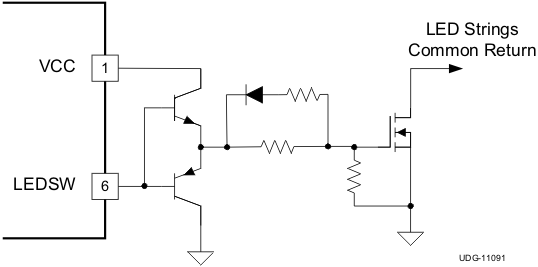 Figure 26. Recommended LED Switch MOSFET Drive Circuit
9.2.2.9 DSR (Dimming Slew Rate)
The DSR pin is used to control the rise and fall time of the VCO control voltage. The DSR capacitor value can be determined by Equation 11. The effective rise time of the LLC primary current is when VDSR is between the 0.9-V gate-drive enable voltage and the VICOMP operating point.

where
- TSLEW is the desired LLC current rise and fall time
- VICOMP_REG is the ICOMP voltage regulation point
Because the DSR voltage starts at 0 V and the LLC gate-drive enable is typically 0.9 V, there is a delay from the DIM rising edge and LEDSW rising edge until the LLC gate drivers are enabled. An easy solution to eliminate a majority of the delay is to use a resistor in series with CDSR. Because DSR is clamped at a Vbe above VICOMP, the recommended resistance is 15 kΩ to 17 kΩ to provide a 640-mV to 720-mV initial voltage delta.
9.2.2.10 DTY (Dimming Duty-Cycle Average)
The DTY pin generates a voltage inversely proportional to the DIM duty-cycle with a 100-mV offset. The voltage range is 100 mV to 2.6 V corresponding to 100% dimming and 0% dimming. This voltage is compared to the DADJ rising ramp to determine the dimming duty-cycle compensation delay time.
The capacitor value is selected to provide low ripple voltage at the DIM frequency. A good guideline is to target 100 V or less peak-to-peak ripple voltage. There is a trade-off of DTY capacitor value and response to DIM duty-cycle transients. For faster response time to significant changes in DIM duty-cycle select a lower value capacitance. Equation 12 can be used to select a DTY capacitor based on maximum ripple voltage and DIM frequency.

where
- FDIM is the dimming frequency
- VDTY(pp) is the maximum peak to peak ripple voltage.
Equation 13 can be used to determine the average of VDTY at any given DIM duty-cycle.

where
9.2.2.11 DADJ (Dimming Duty-Cycle Adjust)
The DADJ pin is a 20-µA current source enabled at the DIM falling edge. The capacitor connected to this pin determines the slope of VDADJ. LLC-OFF is the internal signal that controls the turnon and turnoff of the LLC power stage. The rising edge of LLC-OFF corresponds to a falling edge at the DIM input. The falling edge of the LLC-OFF signal is delayed until the rising edge of the DADJ voltage crosses the voltage on DTY. See Dimming Operation discussion for more details.
An initial value DADJ capacitor can be determined by Equation 14. The dimming performance at lowest DIM on time must be evaluated as described in the following paragraph.

where
- DIMDMIN is the minimum dimming duty cycle
- FDIM is the dimming frequency
- TRISE is the effective DSR rise time
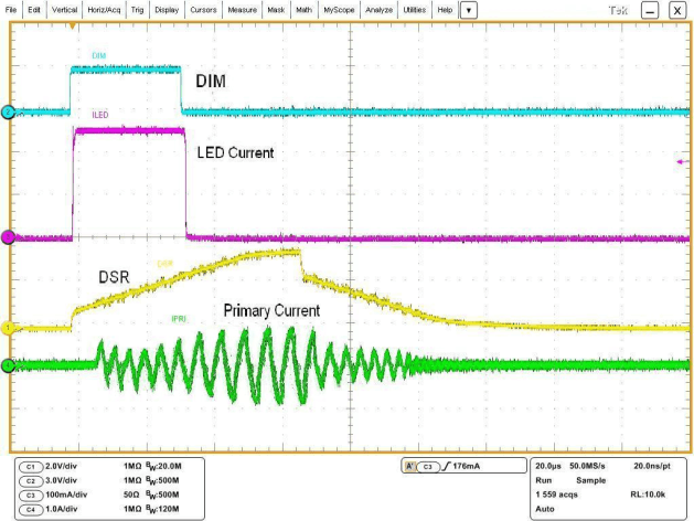
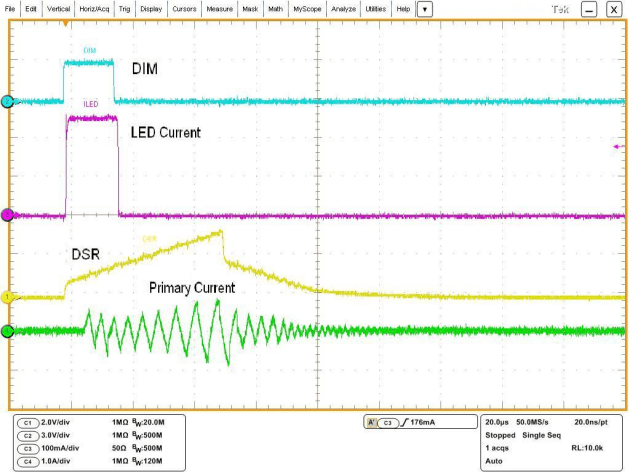
To ensure consistent LED current regulation during DIM duty-cycle transients, it is important to confirm that ICOMP achieves the steady-state operating voltage at the lowest DIM duty-cycle. Because DSR is clamped a VBE (approximately 0.7 V) above ICOMP, this signal can be inspected to confirm a steady-state operating point is achieved after the programmed DSR rise time. Confirm that the DSR signal achieves a relatively flat voltage during the lowest DIM duty-cycle condition. Figure 27 and Figure 28 below are scope plots of 1% DIM duty-cycle where DSR reaches the steady-state operating point, and 0.5% DIM where DSR is still rising and ICOMP is open loop. If DSR is still rising during the lowest DIM duty cycle, increase the DADJ capacitor value until DSR achieves a relatively flat response as shown in Figure 27, the 1% DIM duty-cycle scope plot below.
9.2.2.12 OV (Output Overvoltage)
The OV pin is connected to an output-voltage sense resistor divider with oring diodes to all of the LED outputs. The OV threshold is 2.6 V with 240-mV hysteresis. During an OV fault the GD1 and GD2 gate drivers are disabled and the LEDSW goes low (off). When the OV fault clears, the soft-start cycle is initiated.
A configuration is shown in Figure 29 below that allows for summing of multiple LED string outputs into common UV and OV dividers. Consider the total resistance of the divider networks because the divider bias current is provided by the highest voltage LED string. Equation 15 and Equation 16 can be used to determine total divider resistance and each component values.

where
- VOUT is LED string voltage
- IOUT is LED DC output current
- DMIN is minimum dimming duty-cycle
- IMATCH is LED current matching target
- OV and UV dividers are approximately equal resistance

where
- VOVLO is the OVP threshold
- VD is the summing diode voltage drop
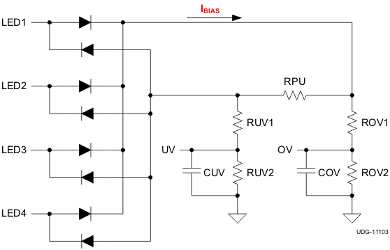 Figure 29. Application of Overvoltage and Undervoltage
9.2.2.13 UV (Output Undervoltage)
UV is connected to an output-voltage sample of the converter. The UV threshold is 2.4 V with 240-mV hysteresis. UV below 2.4 V is considered an undervoltage fault which disables the GD1 and GD2 gate drivers, LEDSW output goes low, the 10-ms soft-start clamp and soft-start cycle are initiated. The UV comparator is disabled until SS voltage is 4.2 V to allow the output capacitors to charge to the normal operating voltage during start-up of the converter.
See the OV and UV divider diagram above for a typical configuration that allows for summing of multiple LED string outputs into common UV and OV dividers. Consider the value of RPU to avoid a current path from the highest voltage LED string to the lowest voltage LED string. Equation 17, Equation 18, and Equation 19 assume a 2× VOUT delta as the maximum UVLO voltage.

where
- LED voltage total tolerance is ±5%
- OV and UV dividers are approximately equal resistance


where
- VUVLO is the UVP threshold
- VD is the summing diode voltage drop
9.2.2.14 CL (Current Limit)
The CL pin is typically connected to the rectified and filtered output of a primary current sense transformer. There are two levels of current limit protection: restart and latching. When CL exceeds 0.95 V the gate drivers are disabled and LEDSW goes low, when the CL voltage reduces to 475 mV the soft-start cycle is initiated. If CL exceeds a 1.9-V threshold, the gate drivers are disabled and LEDSW goes low, this condition is latched until VCC is recycled below the UVLO threshold.
9.2.3 Application Curves
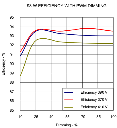 Figure 30. Efficiency 10% to 100% PWM Dimming
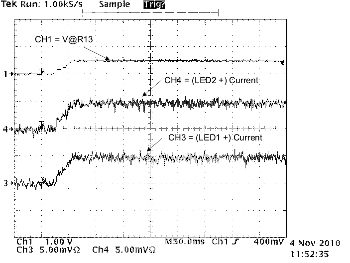 Figure 32. Current LED1 (CH3) and LED2 (CH4)
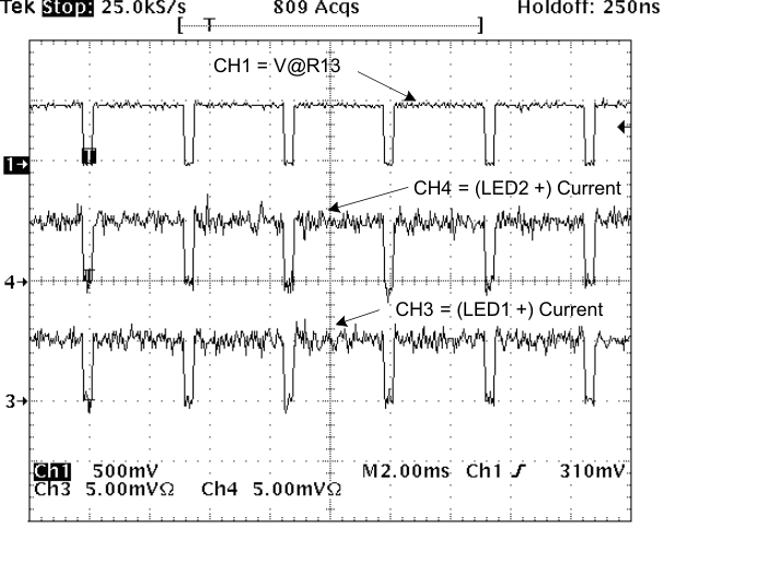 Figure 34. Current LED1 (CH3) and LED2 (CH4)
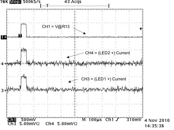 Figure 36. Current LED1 (CH3) and LED2 (CH4)
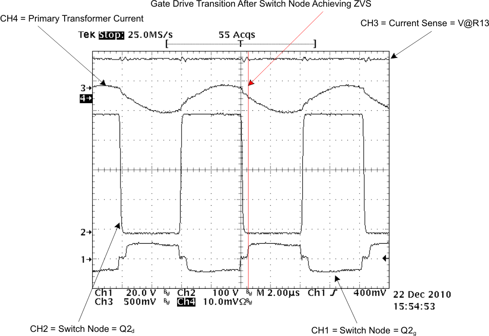
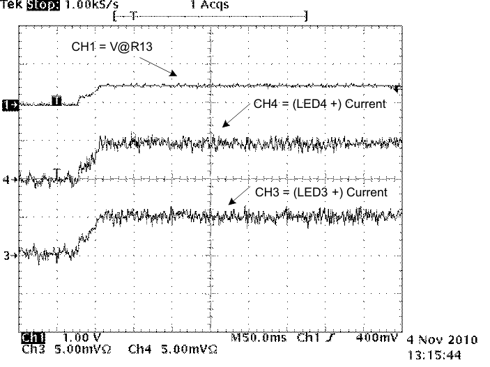 Figure 33. Current LED3 (CH3) and LED4 (CH4)
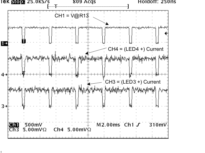 Figure 35. Current LED3 (CH3) and LED4 (CH4)
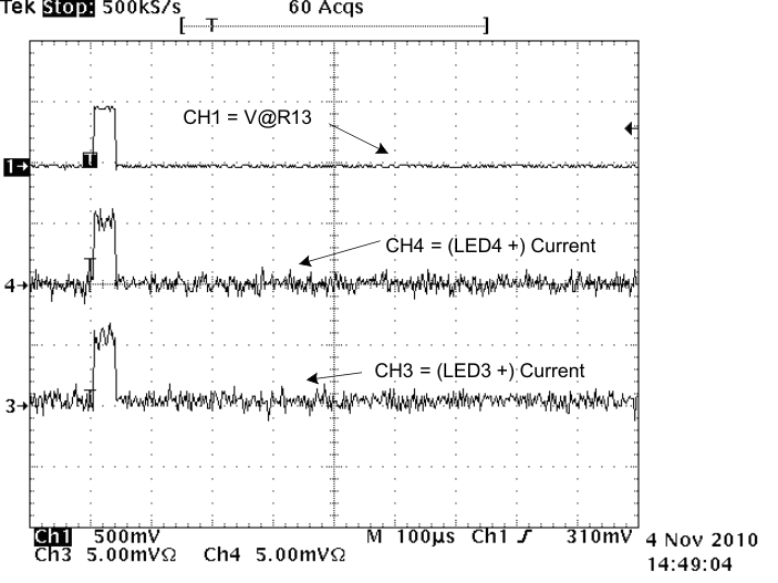 Figure 37. Current LED3 (CH3) and LED4 (CH4)