SLUSAD7B April 2011 – July 2016 UCC25710
PRODUCTION DATA.
- 1 Features
- 2 Applications
- 3 Description
- 4 Revision History
- 5 Description (continued)
- 6 Pin Configuration and Functions
- 7 Specifications
- 8 Detailed Description
-
9 Application and Implementation
- 9.1 Application Information
- 9.2
Typical Application
- 9.2.1 Design Requirements
- 9.2.2
Detailed Design Procedure
- 9.2.2.1 Determining Transformer and Resonant Circuit Parameters
- 9.2.2.2 CS (Output Current Sense)
- 9.2.2.3 ICOMP (Current Amplifier Compensation)
- 9.2.2.4 SS (Soft Start)
- 9.2.2.5 FMAX (Maximum VCO Frequency)
- 9.2.2.6 FMIN (Minimum VCO Frequency)
- 9.2.2.7 GD1 and GD2 (Gate Drive 1 and 2)
- 9.2.2.8 LEDSW (LED Switch Drive)
- 9.2.2.9 DSR (Dimming Slew Rate)
- 9.2.2.10 DTY (Dimming Duty-Cycle Average)
- 9.2.2.11 DADJ (Dimming Duty-Cycle Adjust)
- 9.2.2.12 OV (Output Overvoltage)
- 9.2.2.13 UV (Output Undervoltage)
- 9.2.2.14 CL (Current Limit)
- 9.2.3 Application Curves
- 10Power Supply Recommendations
- 11Layout
- 12Device and Documentation Support
- 13Mechanical, Packaging, and Orderable Information
Package Options
Mechanical Data (Package|Pins)
- DW|20
Thermal pad, mechanical data (Package|Pins)
Orderable Information
8 Detailed Description
8.1 Overview
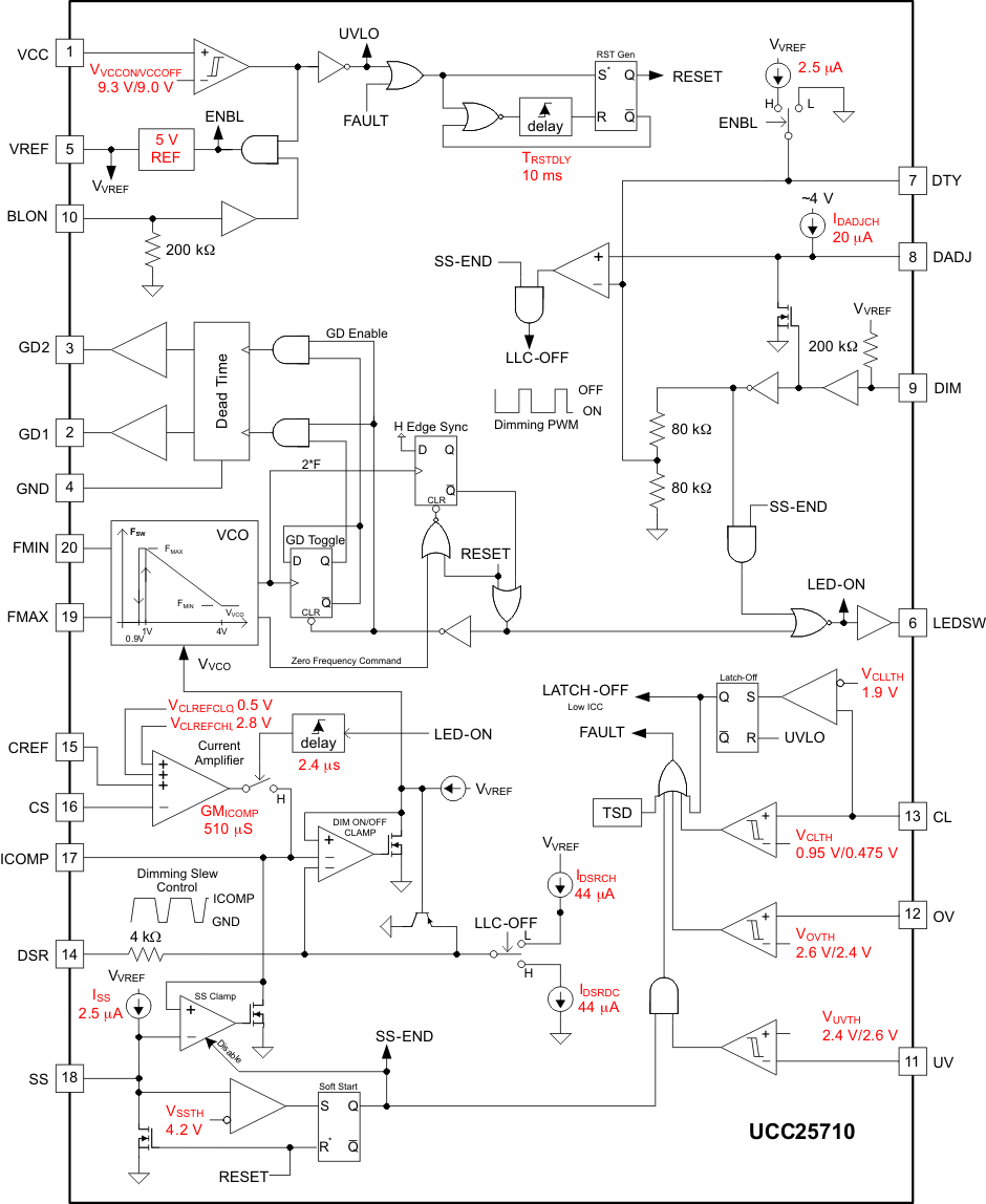
The UCC25710 is a highly integrated LLC controller designed specifically for multi-string LED lighting applications. The half-bridge LLC control is combined with independent PWM dimming or non-dimming of the LED current for control of the light output.
The UCC25710 is designed to provide power from a high voltage DC bus, such as the output from a PFC stage. Input over current-sensing protects the system in the event of a fault and gate drive outputs provide the drive signals to the LLC stage. Output overvoltage and undervoltage provide additional protection. LED current is sensed with a resistor in series with the LED’s. The UCC25710 has separate enable and dimming inputs.
This arrangement of a multi-transformer architecture, as shown in Figure 25, results in a highly efficient power supply.
8.2 Functional Block Diagram
8.3 Feature Description
Signal names and pin functions are depicted in Functional Block Diagram.
8.3.1 Multi-transformer Architecture
The multi-transformer LED driver architecture is a very attractive solution for driving multiple LED strings at the same current using a single power train and control device. Excellent LED string current matching from string to string (<1%) excellent LED current linearity from 1% to 100% dimming (<2%), and high efficiency can be achieved (>94%). Because this architecture is intended to use the 400-V output of the PFC stage, there is a significant cost advantage over typical LED backlight implementations because a power stage can be eliminated.
The architecture and UCC25710 control device are based on the LLC resonant half-bridge topology. The controller feedback loop is configured to regulate the total LED current typically with a current-sense resistor. The arrangement of the transformers with the primaries in series provides excellent LED string current matching. Because the primaries are in series, the current in each transformer primary is the same. The secondary current is the primary current times the turns ratio. The net primary magnetizing current is circulated in the primary side of the half bridge and does not affect the current transferred to the outputs. In each transformer, differences in magnetizing current caused by different magnetizing inductance or winding voltage will cause a difference in current transferred to the LED outputs, although the difference in transferred current is minimal with typical transformer tolerances and following the guidance in the Determining Transformer and Resonant Circuit Parameters below.
The UCC25710 includes all of the functions necessary to implement a total LED backlight driver including GM current amplifier, VCO, reference regulator, soft start, dimming duty cycle compensation and protection for OV, UV, current limit, and thermal shutdown. There are additional features to minimize audible noise during dimming and provide fast LED current rise and fall times.
8.3.2 Start-Up and Non-Dimming Operation
The UCC27510 is enabled when VCC exceeds the VVCCON threshold and BLON is high. At this time the soft-start cycle is initiated following a 10-ms reset delay. A 2.5-µA current source charges the capacitor connected to the SS pin to generate the soft-start ramp. During the soft-start cycle the current amplifier output (ICOMP) is clamped to be equal to or less than SS voltage. The voltage on ICOMP controls the VCO. VICOMP achieves the steady state operating point to regulate the total LED current during the soft-start rise time. The DIM input and the UV input are disabled during soft start to allow the output capacitors to charge to the steady-state operating voltage. When the SS pin reaches the VSSTH threshold the SS-END signal transitions high indicating the end of the soft-start cycle. At this time the UV comparator and DIM input are enabled. See Figure 17 for the timing relationship during soft start.
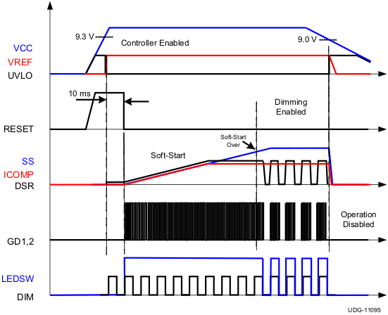 Figure 17. Start-Up Timing Diagram
8.3.3 Dimming Operation
Once the soft-start cycle is complete, the LEDSW output and control of the VCO depend on the DIM input. The dimming input signal controls the LEDSW output maintaining an accurate ON-time relationship between the DIM pulse width and LED current pulse width; the internal control signal is LED-ON. The LED-ON signal also controls a switch between the GM current amplifier output and the ICOMP pin. On the DIM rising edge the switch from the amplifier to the ICOMP pin is turned on after a 2.4-µs delay. The small delay time allows time to turn on the LED switch MOSFET. On the DIM falling edge the switch between the GM amplifier is turned off. During the DIM OFF-time the compensation capacitor at the ICOMP pin holds the correct steady-state operating voltage for the current loop. It is important that any DC loading of this pin is kept to an absolute minimum or current errors results as the dimming duty-cycle is reduced.
The LLC power stage is gated on and off during dimming with the dimming input signal. The UCC25710 allows control of the slew rate of the LLC power delivery at the rising and falling edges of a dim cycle allowing potentially audible electro-mechanically induced noise to be minimized. In addition, the falling, or turnoff, edge of a dimming cycle can be delayed, allowing the current loop to maintain control at low dimming duty-cycles even when the ramp rates have been slowed. See Figure 18.
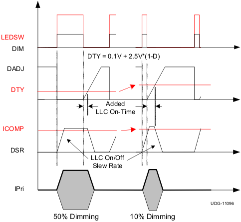 Figure 18. Dimming Timing Diagram
The power through the LLC converter is inversely proportional to the frequency of the VCO. The VCO frequency, in turn, is inversely proportional to the VCO control signal. See Figure 19 for details of this relationship. The dimming input generates an LLC-OFF signal that is used to select either a charging or discharging state for a capacitor applied to the DSR pin. The ±44 µA of current and associated capacitor set a ramp rate for the rise and fall of the DSR voltage. The control voltage to the VCO is dominated by the DSR voltage when the DSR voltage is less than the ICOMP pin – allowing the falling ramp on the DSR pin to softly turnoff the LLC power stage and softly return it to the same operating state as it rises.
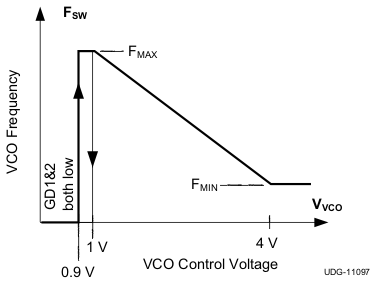 Figure 19. VCO Characteristics
The LLC-OFF signal is an inverted version of the dimming input signal. The falling edge of LLC-OFF is synchronized with the rising edge of the DIM signal. At a negative DIM edge the DADJ and DTY signals are combined to delay the rising edge of LLC-OFF providing a duty-cycle compensation time that is a function of the dimming duty cycle.
Averaged by a capacitor at the DTY pin, the voltage on DTY is inversely proportional to the dimming duty cycle; the voltage is
where
- D is the dimming PWM duty-cycle
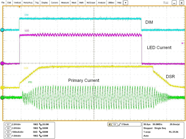
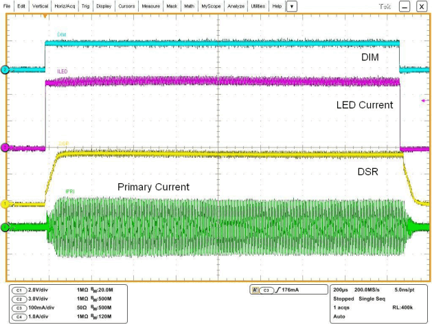
The DTY voltage range is 100 mV at 100% DIM duty-cycle, or LED current continuously on, to 2.6 V at 0% DIM duty cycle, or LED current continuously off. The DADJ pin 20-µA current source is allowed to charge the pin capacitor after a DIM falling edge. The LLC-OFF signal transitions high when the capacitor on DADJ charges to the voltage on DTY. See Figure 18 for the timing relationship during dimming. The scope plots in Figure 20 and Figure 21 below show an example LED driver at 10% and 50% DIM duty cycle.
8.3.4 Fault Condition Operation
The UCC25710 has a similar response to overvoltage, thermal shutdown and current limit faults. Figure 22 shows the fault response. The OV input has a 2.6-V threshold and 240 mV of hysteresis. When OV is above 2.6 V the internal FAULT signal is active which results in the RESET signal going high. With RESET high the gate drivers are disabled, the SS pin is discharged to ground, and the LEDSW output is turned off. When OV is below 2.36 V the FAULT signal is inactive which starts the 10-ms SS clamp timer.
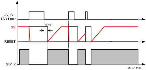 Figure 22. OV, CL(1 V) and TSD Fault Timing Diagram
RESET is extended 10 ms beyond FAULT going low. After the 10-ms soft-start timer the normal soft-start sequence begins. Thermal shutdown generates the same internal FAULT signal when the internal temperature reaches 160°C and a restart sequence begins after the junction temperature drops by the 25°C of threshold hysteresis.
The current limit comparator has two thresholds. The lower threshold of 0.95 V results in a shutdown and restart as described for OVP, the OC pin has 0.475 V of hysteresis. The second current limit threshold of 1.9 V results in a latch-off fault. VCC must be recycled below the VCCOFF threshold to reset the latched OC fault.
The undervoltage fault has a different response to allow the converter to charge the output capacitors in a normal start-up condition. Because UV is disabled during soft start, a sustained UV fault results in a 10-ms soft-start clamp time plus the time required for the SS pin to charge to VSSTH which is 4.15 V. See Figure 23 for UV fault condition timing diagrams.
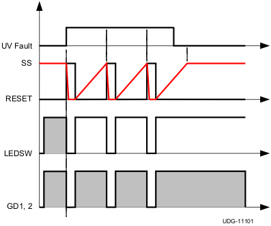 Figure 23. UV Fault Timing Diagram
8.4 Device Functional Modes
The device has two functional modes: non-dimming and dimming.
In the non-dimming mode the DIM input pin is held high (above 1.5 V typically)
In the dimming mode the DIM pin is switched between high and low levels.
The dimming slew rate controls the rate of change between the high and low LED currents.
This is set with a capacitor on the DSR input pin.
Additionally, a capacitor on the DADJ input pin extends the falling edges of the dimming cycle.
This allows for control at very low dimming ratios.