SLUSAD7B April 2011 – July 2016 UCC25710
PRODUCTION DATA.
- 1 Features
- 2 Applications
- 3 Description
- 4 Revision History
- 5 Description (continued)
- 6 Pin Configuration and Functions
- 7 Specifications
- 8 Detailed Description
-
9 Application and Implementation
- 9.1 Application Information
- 9.2
Typical Application
- 9.2.1 Design Requirements
- 9.2.2
Detailed Design Procedure
- 9.2.2.1 Determining Transformer and Resonant Circuit Parameters
- 9.2.2.2 CS (Output Current Sense)
- 9.2.2.3 ICOMP (Current Amplifier Compensation)
- 9.2.2.4 SS (Soft Start)
- 9.2.2.5 FMAX (Maximum VCO Frequency)
- 9.2.2.6 FMIN (Minimum VCO Frequency)
- 9.2.2.7 GD1 and GD2 (Gate Drive 1 and 2)
- 9.2.2.8 LEDSW (LED Switch Drive)
- 9.2.2.9 DSR (Dimming Slew Rate)
- 9.2.2.10 DTY (Dimming Duty-Cycle Average)
- 9.2.2.11 DADJ (Dimming Duty-Cycle Adjust)
- 9.2.2.12 OV (Output Overvoltage)
- 9.2.2.13 UV (Output Undervoltage)
- 9.2.2.14 CL (Current Limit)
- 9.2.3 Application Curves
- 10Power Supply Recommendations
- 11Layout
- 12Device and Documentation Support
- 13Mechanical, Packaging, and Orderable Information
Package Options
Mechanical Data (Package|Pins)
- DW|20
Thermal pad, mechanical data (Package|Pins)
Orderable Information
11 Layout
11.1 Layout Guidelines
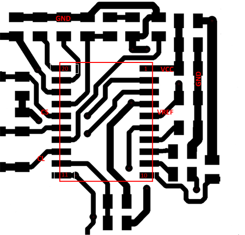
As with all PWM controllers, the effectiveness of the filter capacitors on the signal pins depends upon the integrity of the ground signal. Separating the high di/dt induced noise on the power ground from the low current quiet signal ground is required for adequate noise immunity. As shown Figure 38, the bypass capacitors on VCC and VREF have one end located in close proximity to their associated pins and the other ends are returned directly to the GND pin or to the portion of the ground plane associated with the low level GND signal and not to the high current power return. Low-ESR type ceramic capacitors are recommended as bypass capacitors.
The gate-drive output signals (GD1 and GD2) can cause interference on the low-level inputs (CL and CS) and for this reason must be routed as far as possible away from them and have short direct paths to the gate-drive transformer. In general any slow-changing analog signals must be routed away from high-speed digital signals.
Timing resistors FMIN and FMAX must be placed as close as possible to the pins on the UCC25710.
11.2 Layout Example
 Figure 38. Layout Example for UCC25710