SLUSCW3 August 2017 UCC27712-Q1
PRODUCTION DATA.
- 1 Features
- 2 Applications
- 3 Description
- 4 Simplified Schematic
- 5 Revision History
- 6 Pin Configuration and Functions
- 7 Specifications
- 8 Detailed Description
-
9 Application and Implementation
- 9.1 Application Information
- 9.2
Typical Application
- 9.2.1 Design Requirements
- 9.2.2
Detailed Design Procedure
- 9.2.2.1 Selecting HI and LI Low Pass Filter Components (RHI, RLI, CHI, CLI)
- 9.2.2.2 Selecting Bootstrap Capacitor (CBOOT)
- 9.2.2.3 Selecting VDD Bypass/Holdup Capacitor (CVDD) and Rbias
- 9.2.2.4 Selecting Bootstrap Resistor (RBOOT)
- 9.2.2.5 Selecting Gate Resistor RON/ROFF
- 9.2.2.6 Selecting Bootstrap Diode
- 9.2.2.7 Estimate the UCC27712-Q1 Power Losses (PUCC27712-Q1)
- 9.2.2.8 Estimating Junction Temperature
- 9.2.2.9 Operation With IGBT's
- 9.2.3 Application Curves
- 10Power Supply Recommendations
- 11Layout
- 12Device and Documentation Support
- 13Mechanical, Packaging, and Orderable Information
Package Options
Mechanical Data (Package|Pins)
- D|8
Thermal pad, mechanical data (Package|Pins)
Orderable Information
8 Detailed Description
8.1 Overview
The UCC27712-Q1 consists of one ground-referenced channel (LO) and one floating channel (HO) which is designed for operating with bootstrap or isolated power supplies. The device features fast propagation delays and excellent delay matching between both channels. On the UCC27712-Q1, each channel is controlled by its respective input pins,
Developed with TI’s state of the art high-voltage technology, the device features robust drive with excellent noise and transient immunity including large negative voltage tolerance on its inputs, high dv/dt tolerance, and wide negative transient safe operating area (NTSOA) on the switch node (HS).
The UCC27712-Q1 includes protection features where the outputs are held low when the inputs are floating or when the minimum input pulse width specification is not met. Interlock and deadtime functions prevent both outputs from being turned on simultaneously. In addition, the device accepts a wide range bias supply range from 10 V ~ 22 V, and offers UVLO protection for both the VDD and HB bias supply.
High-current, gate-driver devices are required in switching power applications for a variety of reasons. In order to implement fast switching of power devices and reduce associated switching power losses, a powerful gate-driver device is employed between the PWM output of control devices and the gates of the power semiconductor devices. Further, gate-driver devices are indispensable when having the PWM controller device directly drive the gates of the switching devices is sometimes not feasible. In the case of digital power supply controllers, this situation is often encountered because the PWM signal from the digital controller is often a 3.3-V logic signal which is not capable of effectively turning on a power switch.
In bridge topologies, like hard-switch half bridge, hard-switch full bridge, half-bridge and full-bridge LLC, and phase-shift full bridge, the source and emitter pin of the top-side power MOSFET and IGBT switch is referenced to a node whose voltage changes dynamically; that is, not referenced to a fixed potential, so floating-driver devices are necessary in these topologies.
The UCC27712-Q1 is a high-side and low-side driver dedicated for offline AC-to-DC power supplies and inverters. The high side is a floating driver that can be biased effectively using a bootstrap circuit, and can handle up to 600-V. The driver can be used with 100% duty cycle as long as HB-HS can be above UVLO of the high side.
The device features industry best-in-class propagation delay and delay matching between both channels aimed at minimizing pulse width distortion in high-frequency switching applications. Each channel is controlled by its respective input pins (HI and LI), allowing independent flexibility to control on and off state of the output but does not allow the HO and LO outputs to be on at the same time. The UCC27712-Q1 includes an interlock feature which guarantees a 150ns dead time between the HO and LO outputs if the HI and LI inputs are complimentary. The UCC27712-Q1 includes protection features wherein the outputs are held low when inputs are floating or when the minimum input pulse width specification is not met. The driver inputs are CMOS and TTL compatible for easy interface to digital power controllers and analog controllers alike.
8.2 Functional Block Diagram
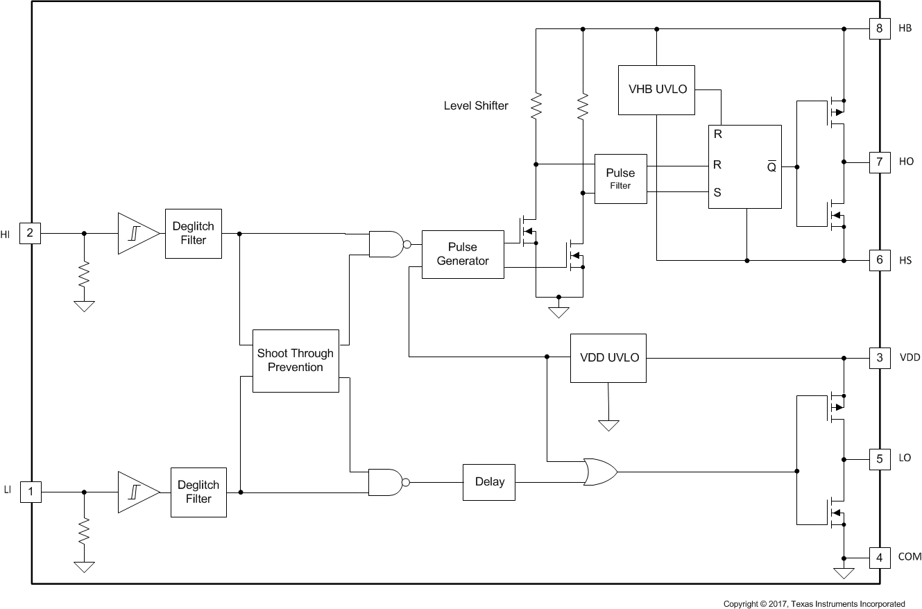 Figure 29. UCC27712-Q1 Block Diagram
8.3 Feature Description
8.3.1 VDD and Under Voltage Lockout
The UCC27712-Q1 has an internal under voltage-lockout (UVLO) protection feature on the supply circuit blocks between VDD and VSS pins, as well as between HB and HS pins. When VDD bias voltage is lower than the VVDD(on) threshold at device start-up or lower than VVDD(off) after start-up, the VDD UVLO feature holds both the LO and HO outputs low, regardless of the status of the HI and LI inputs. On the other hand, if HB-HS bias supply voltage is lower than the VVHB(on) threshold at start-up or VVHB(off) after start-up, the HB-HS UVLO feature only holds HO to low, regardless of the status of the HI. The LO output status is not affected by the HB-HS UVLO feature (see Table 1 and Table 2). This allows the LO output to turn-on and re-charge the HB-HS capacitor using the boot-strap circuit and thus allows HB-HS bias voltage to surpass the VVHB(on) threshold.
Both the VDD and VHB UVLO protection functions are provided with a hysteresis feature. This hysteresis prevents chatter when there is ground noise from the power supply. Also this allows the device to accept a small drop in the bias voltage which is bound to happen when the device starts switching and quiescent current consumption increases instantaneously, as well as when the boot-strap circuit charges the HB-HS capacitor during the first instance of LO turn-on causing a drop in VDD voltage.
The UVLO circuit of VDD-VSS and HB-HS in UCC27712-Q1 generate internal signals to enable/disable the outputs after UVLO_ON/UVLO_OFF thresholds are crossed respectively (please refer to Figure 30). Design considerations indicate that the UVLO propagation delay before the outputs are enabled and disabled can vary from 20 μs to 50 μs.
Table 1. VDD UVLO Feature Logic Operation
| CONDITION (VHB-VHS>VVHB, ON FOR ALL CASES BELOW) | HI | LI | HO | LO |
|---|---|---|---|---|
| VDD-VSS < VVDD(on) during device start up | H | L | L | L |
| VDD-VSS < VVDD(on) during device start up | L | H | L | L |
| VDD-VSS < VVDD(on) during device start up | H | H | L | L |
| VDD-VSS < VVDD(on) during device start up | L | L | L | L |
| VDD-VSS < VVDD(off) after device start up | H | L | L | L |
| VDD-VSS < VVDD(off) after device start up | L | H | L | L |
| VDD-VSS < VVDD(off) after device start up | H | H | L | L |
| VDD-VSS < VVDD(off) after device start up | L | L | L | L |
Table 2. VHB UVLO Feature Logic Operation
| CONDITION (VDD-VSS > VVDD,ON FOR ALL CASES BELOW) | HI | LI | HO | LO |
|---|---|---|---|---|
| VHB-VHS < VVHB(on) during device start up | H | L | L | L |
| VHB-VHS < VVHB(on) during device start up | L | H | L | H |
| VHB-VHS < VVHB(on) during device start up | H | H | L | L |
| VHB-VHS < VVHB(on) during device start up | L | L | L | L |
| VHB-VHS < VVHB(off) after device start up | H | L | L | L |
| VHB-VHS < VVHB(off) after device start up | L | H | L | H |
| VHB-VHS < VVHB(off) after device start up | H | H | L | L |
| VHB-VHS < VVHB(off) after device start up | L | L | L | L |
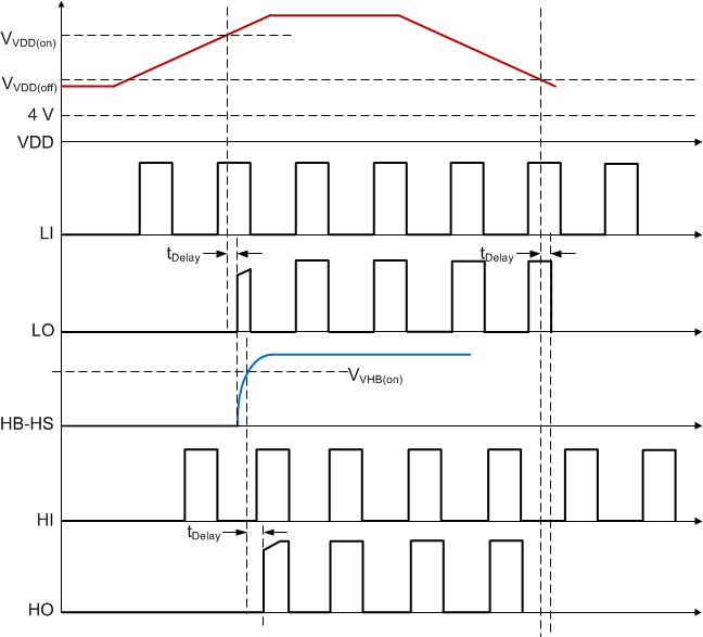 Figure 30. Power-Up Driver
8.3.2 Input and Output Logic Table
UCC27712-Q1 features separate inputs, HI and LI, for controlling the state of the outputs, HO and LO, respectively. The device does include internal cross-conduction prevention logic and does not allow both HO and LO outputs to be turned on simultaneously (refer to Table 3). This feature prevents cross conduction in bridge topologies in the case of incorrect timing from the controller.
Table 3. Input/Output Logic Table
(Assuming no UVLO fault condition exists for VDD and VHB)
| HI | LI | HO | LO | Note | |
|---|---|---|---|---|---|
| L | L | L | L | ||
| L | H | L | H | Output transitions occur after the dead time expires | |
| H | L | H | L | ||
| H | H | L | L | ||
| Left Open | Left Open | L | L | ||
8.3.3 Input Stage
The input pins of UCC27712-Q1 are based on a TTL and CMOS compatible input-threshold logic that is independent of the VDD supply voltage. With typical high threshold (VINH) of 2.0 V and typical low threshold (VINL) of 1.2 V, along with very little temperature variation as summarized in Figure 16 and Figure 17, the input pins are conveniently driven with logic level PWM control signals derived from 3.3-V and 5-V digital power-controller devices. Wider hysteresis (typically 0.8 V) offers enhanced noise immunity compared to traditional TTL logic implementations, where the hysteresis is typically less than 0.5 V. UCC27712-Q1 also features tight control of the input pin threshold voltage levels which eases system design considerations and ensures stable operation across temperature.
The UCC27712-Q1 includes an important feature: wherein, whenever any of the input pins is in a floating condition, the output of the respective channel is held in the low state. This is achieved using COM pull-down resistors on all the input pins (HI, LI).
The UCC27712-Q1 input pins are capable of sustaining voltages higher than the bias voltage applied on the VDD pin of the device, as long as the absolute magnitude is less than the recommended operating condition's maximum ratings. This features offers the convenience of driving the PWM controller at a higher VDD bias voltage than the UCC27712-Q1 helping to reduce gate charge related switching losses. This capability is envisaged in UCC27712-Q1 by way of two ESD diodes tied back-to-front as shown in Figure 31.
Additionally, the input pins are also capable of sustaining negative voltages below COM, as long as the magnitude of the negative voltage is less than the recommended operating condition minimum ratings. A similar diode arrangement exists between the input pins and COM as illustrated in Figure 31.
The input stage of each driver must be driven by a signal with a short rise or fall time. This condition is satisfied in typical power supply applications, when the input signals are provided by a PWM controller or logic gates with fast transition times. With a slow changing input voltage, the output of driver may switch repeatedly at a high frequency. While the wide hysteresis offered in UCC27712-Q1 definitely alleviates this concern over most other TTL input threshold devices, extra care is necessary in these implementations. If limiting the rise or fall times to the power device is the primary goal, then an external resistance is highly recommended between the output of the driver and the power device. This external resistor has the additional benefit of reducing part of the gate-charge related power dissipation in the gate-driver device package and transferring it into the external resistor itself. If an RC filter is to be added on the input pins for reducing the impact of system noise and ground bounce, the time constant of the RC filter is recommended to be 20 ns or less, for example, 50 Ω with 220 pF is an acceptable choice.
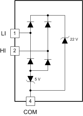 Figure 31. Diode Structure of Input Stage
8.3.4 Output Stage
The UCC27712-Q1 device output stage pull-up structure features a P-Channel MOSFET to provide source current until the output is saturated to VDD or HB. The ROH parameter (see Figure 21) is a DC measurement and it is representative of the on-resistance of the P-Channel device.
The pull-down structure in UCC27712-Q1 is composed of a N-Channel MOSFET. The ROL parameter (see Figure 19), which is also a DC measurement, is representative of the impedance of the pull-down stage in the device.
Each output stage in UCC27712-Q1 is capable of supplying 1.8-A peak source and 2.8-A peak sink current pulses. The output voltage swings between (VDD and COM) / (HB and HS) providing rail-to-rail operation, thanks to the MOSFET output stage which delivers very low drop-out.
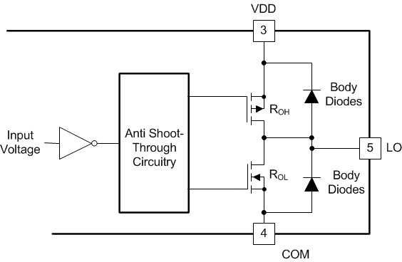 Figure 32. Output Stage Structure
8.3.5 Level Shift
The level shift circuit (refer to the Functional Block Diagram) is the interface from the high-side input to the high-side driver stage which is referenced to the switch node (HS). It is a pulsed generated level shifter. With an input signal the pulse generator generates "on" pulses based on the rising edge of the signal and "off" pulses based on the falling edge. On pulses and off pulses turn on each branch of the level shifter so that current flows in each branch to generate different voltages, which is transferred to the set and reset signal in the high side. The signal is rebuilt by the RS latch in the high side domain. The level shift allows control of the HO output referenced to the HS pin and provides excellent delay matching with the low-side driver. The delay matching of UCC27712-Q1 is summarized in Figure 6 and Figure 7.
The level shifter in UCC27712-Q1 offers best-in-class capability while operating under negative voltage conditions on HS pin. The level shifter is able to transfer signals from the HI input to HO output with only 4-V headroom between HB and COM. Refer to Operation Under Negative HS Voltage Condition for detailed explanations.
8.3.6 Low Propagation Delays and Tightly Matched Outputs
The UCC27712-Q1 features a best in class, 100-ns (typical) propagation delay (refer to Figure 2, Figure 3, Figure 4 and Figure 5 ) between input and output in high voltage 600-V driver, which goes to offer a low level of pulse width distortion for high frequency switching applications.
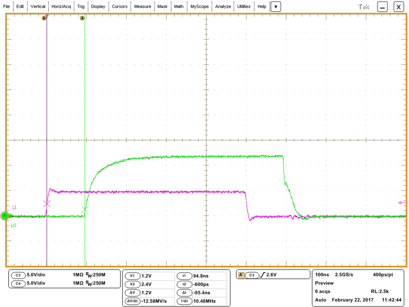 Figure 33. Turn-On Propagation Delay
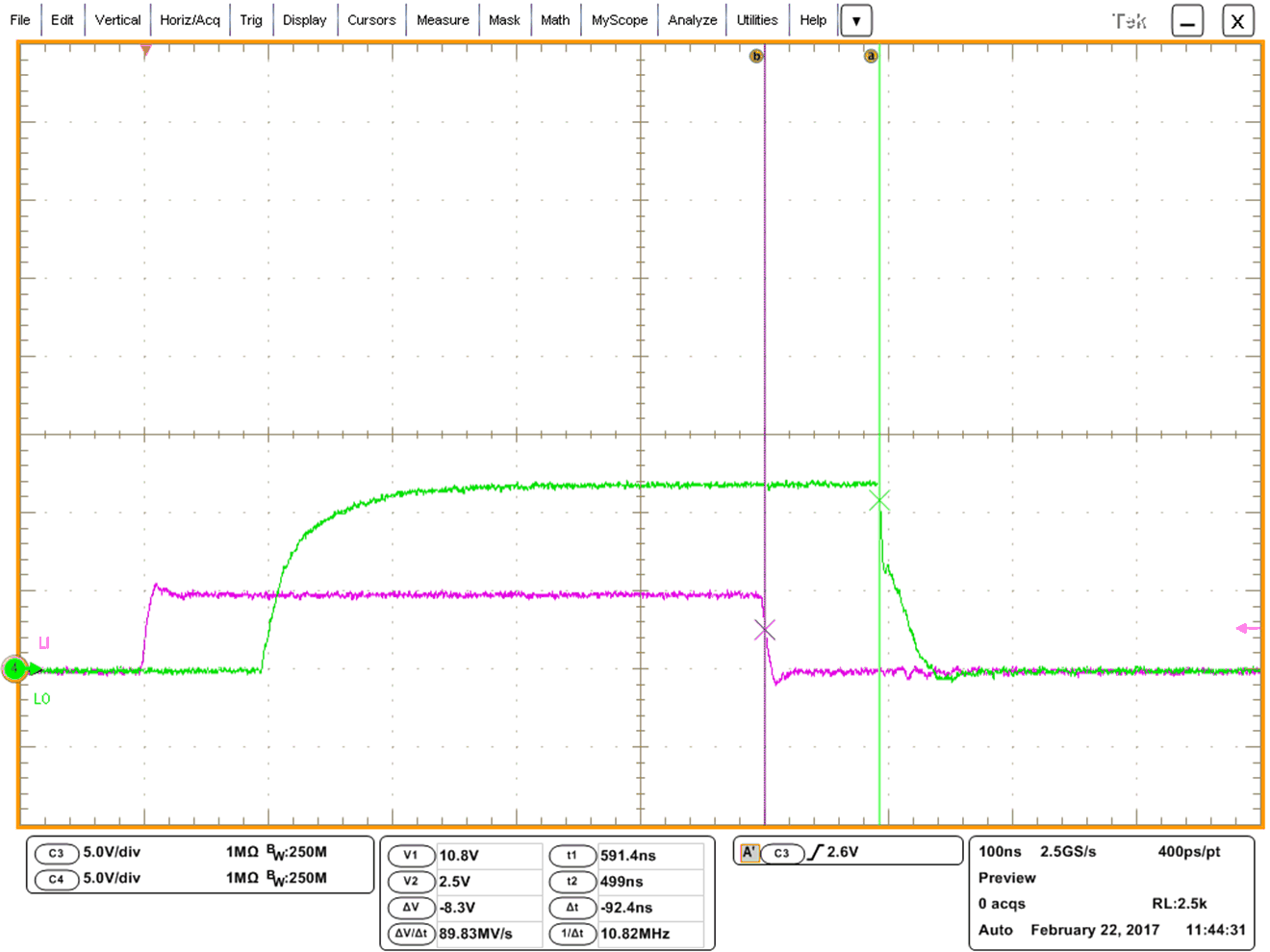 Figure 34. Turn-Off Propagation Delay
8.3.7 Parasitic Diode Structure
Figure 35 illustrates the multiple parasitic diodes involved in the ESD protection components of UCC27712-Q1 device. This provides a pictorial representation of the absolute maximum rating for the device.
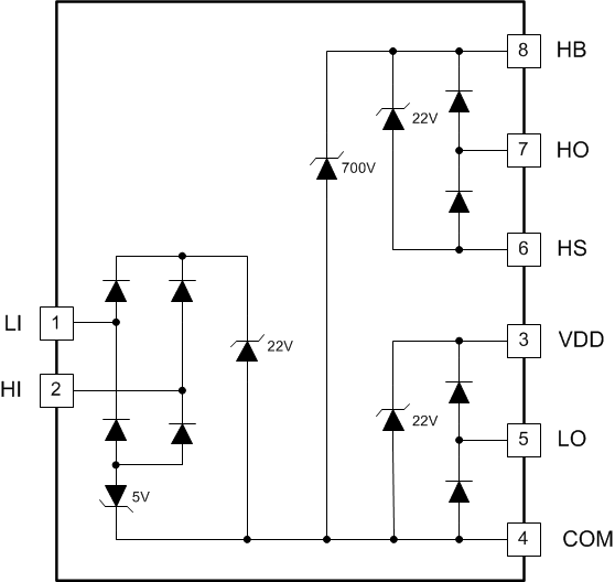 Figure 35. ESD Structure
8.4 Device Functional Modes
8.4.1 Minimum Input Pulse Operation
The UCC27712-Q1 device has a minimum turn-on, turn-off pulse transfer function to the output pin from the input pin. This function ensures UCC27712-Q1 is in the correct state when the input signal is very narrow. The function is summarized in Figure 36 and Figure 37. The tON which is 25 ns typical is shown in Figure 36 and tOFF which is 35ns typical is shown in Figure 37
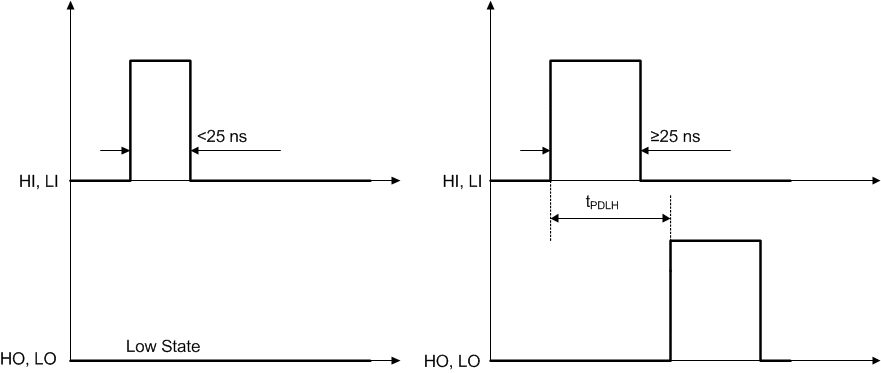 Figure 36. Minimum Turn-On Pulse
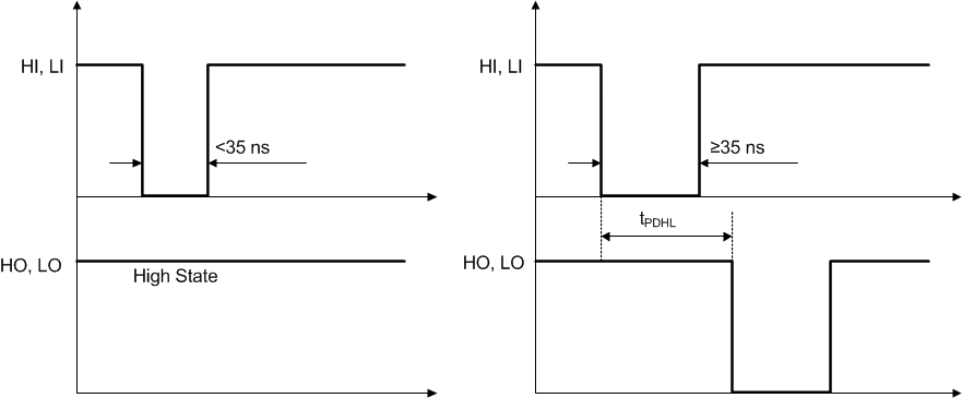 Figure 37. Minimum Turn-Off Pulse
8.4.2 Output Interlock and Dead Time
The UCC27712-Q1 has cross-conduction prevention logic, which is a feature that does not allow both the high-side and low-side outputs to be in high state simultaneously. In bridge power supply topologies, such as half-bridge or full-bridge, the UCC27712-Q1 interlock feature will prevent the high-side and low-side power switches to be turned on simultaneously. The UCC27712-Q1 generates a fixed minimum dead time of tDT which is 150ns nominal in the case of LI and HI overlap or no dead time. Figure 38 illustrates the mode of operation where LI and HI have no dead time and HO and LO outputs have the minimum dead time of tDT.
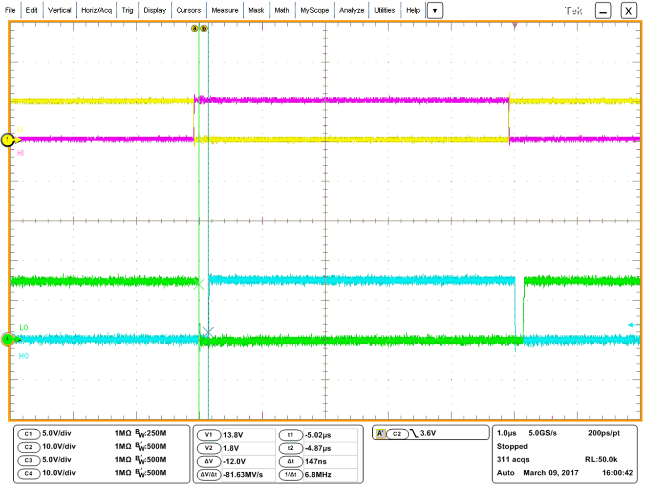 Figure 38. HO and LO Minimum Dead Time with LI HI Complementary
An input signal's falling edge activates the dead time for the other signal. The output signal's dead time is always set to the longer of either the driver's minimum dead time, tDT, or the input signal's own dead time. If both inputs are high simultaneously, both outputs will immediately be set low. This feature is used to prevent cross conduction, and it does not affect the programmed dead time setting for normal operation. Various driver dead time logic operating conditions are illustrated and explained in Figure 39.
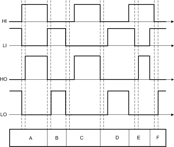 Figure 39. Input and Output Logic Relationship
Condition A: HI goes high, LI goes low. LI sets LO low immediately and assigns tDT to HO. HO is allowed to go high after tDT.
Condition B: LI goes high, HI goes low. HI sets HO low immediately and assigns tDT to HO. LO is allowed to go high after tDT.
Condition C: LI goes low, HI is still low. LI sets LO low immediately and assigns tDT to HO. In this case, the input signal's own dead time is longer than tDT. Thus when HI goes high HO is set high immediately.
Condition D: HI goes low, LI is still low. HI sets HO low immediately and assigns tDT to LO. In this case, the input signal's own dead time is longer than tDT. Thus when LI goes high LO is set high immediately.
Condition E: HI goes high, while LI and LO are still high. To avoid cross-conduction, HI immediately sets LO low and keeps HO low. After some time LI goes low and assigns tDT to HO. LO is already low. After tDT HO is allowed to go high.
Condition F: LI goes high, while HI and HO are still high. To avoid cross-conduction, LI immediately sets HO low and keeps LO low. After some time HI goes low and assigns tDT to LO. HO is already low. After tDT LO is allowed to go high.
8.4.3 Operation Under 100% Duty Cycle Condition
The UCC27712-Q1 allows constant on or constant off operation (0% and/or 100% duty cycle) as long as the VDD and VHB bias supplies are maintained above the UVLO thresholds. This is a challenge when boot-strap supplies are used for VHB. However, when a dedicated bias supply is used, constant on or constant off conditions can be supported. Also consider the HI and LI interlock function prevents both outputs from being high.
8.4.4 Operation Under Negative HS Voltage Condition
A typical half-bridge configuration with UCC27712-Q1 is shown in Figure 40. There are parasitic inductances in the power circuit from die bonding and pinning in QT/QB and PCB tracks of power circuit, the parasitic inductances are labeled LK1,2,3,4.
During switching of HS caused by turning off HO, the current path of power circuit is changed to current path 2 from current path 1. This is known as current commutation. The current across LK3, LK4 and body diode of QB pulls HS lower than COM. The negative voltage of HS with respect to COM causes a logic error of HO if the driver cannot handle negative voltage of HS. However, the UCC27712-Q1 offers robust operation under these conditions of negative voltage on HS.
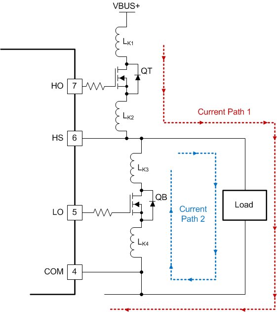 Figure 40. HS Negative Voltage In Half-Bridge Configuration
The level shifter circuit is with respect to COM (refer to Functional Block Diagram), the voltage from HB to COM is the supply voltage of level shifter. Under the condition of HS is negative voltage with respect to COM, the voltage of HB-COM is decreased, as shown in Figure 41. There is a minimum operational supply voltage of level shifter, if the supply voltage of level shifter is too low, the level shifter cannot pass through HI signal to HO. The minimum supply voltage of level shifter of UCC27712-Q1 is 4 V, so the recommended HS specification is dependent on HB-HS. The specification of recommended HS is –11 V at HB – HS = 15 V.
In general, HS can operate until -11 V when HB – HS = 15 V as the ESD structure in Figure 35 allows a maximum voltage difference of 22 V between both pins. If HB-HS voltage is different, the minimum HS voltage changes accordingly.
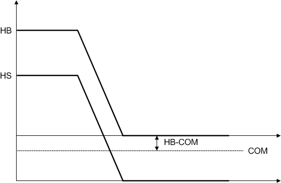 Figure 41. Level Shifter Supply Voltage with Negative HS
NOTE
Logic operational for HS of –11 V to 600 V at HB – HS = 15 V
The capability of a typical UCC27712-Q1 device to operate under a negative voltage condition in HS pin is reported in Figure 43. The test method is shown in Figure 42.
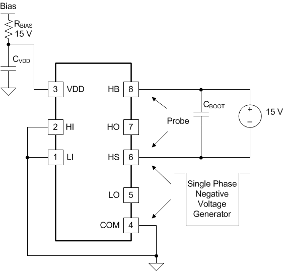 Figure 42. Negative Voltage Test Method
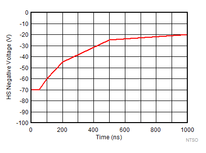 Figure 43. Negative Voltage Chart
 Pulse Width vs Negative Voltage