SLUSCW3 August 2017 UCC27712-Q1
PRODUCTION DATA.
- 1 Features
- 2 Applications
- 3 Description
- 4 Simplified Schematic
- 5 Revision History
- 6 Pin Configuration and Functions
- 7 Specifications
- 8 Detailed Description
-
9 Application and Implementation
- 9.1 Application Information
- 9.2
Typical Application
- 9.2.1 Design Requirements
- 9.2.2
Detailed Design Procedure
- 9.2.2.1 Selecting HI and LI Low Pass Filter Components (RHI, RLI, CHI, CLI)
- 9.2.2.2 Selecting Bootstrap Capacitor (CBOOT)
- 9.2.2.3 Selecting VDD Bypass/Holdup Capacitor (CVDD) and Rbias
- 9.2.2.4 Selecting Bootstrap Resistor (RBOOT)
- 9.2.2.5 Selecting Gate Resistor RON/ROFF
- 9.2.2.6 Selecting Bootstrap Diode
- 9.2.2.7 Estimate the UCC27712-Q1 Power Losses (PUCC27712-Q1)
- 9.2.2.8 Estimating Junction Temperature
- 9.2.2.9 Operation With IGBT's
- 9.2.3 Application Curves
- 10Power Supply Recommendations
- 11Layout
- 12Device and Documentation Support
- 13Mechanical, Packaging, and Orderable Information
Package Options
Mechanical Data (Package|Pins)
- D|8
Thermal pad, mechanical data (Package|Pins)
Orderable Information
7 Specifications
7.1 Absolute Maximum Ratings
Over operating free-air temperature range (unless otherwise noted), all voltages are with respect to COM (unless otherwise noted), currents are positive into and negative out of the specified terminal.(1)| PARAMETER | MIN | MAX | UNIT | ||
|---|---|---|---|---|---|
| Input voltage | HI, LI (2) | –5 | 22 | V | |
| VDD supply voltage | –0.3 | 22 | |||
| HB | –0.3 | 700 | |||
| HB–HS | –0.3 | 22 | |||
| Output voltage | HO | DC | HS–0.3 | HB+0.3 | V |
| Transient, less than 100 ns(3) | HS–2 | HB+0.3 | |||
| LO | DC | –0.3 | VDD+0.3 | V | |
| Transient, less than 100 ns(3) | –2 | VDD+0.3 | |||
| Output current | HO, LO | IOUT_PULSED (100 ns) | 2.8/–1.8 | A | |
| IOUT_DC | 0.15 | ||||
| dVHS/dt | Allowable offset supply voltage transient | –50 | 50 | V/ns | |
| TJ | Junction temperature | –40 | 150 | °C | |
| Tstg | Storage temperature | –65 | 150 | ||
(1) Stresses beyond those listed under Absolute Maximum Ratings may cause permanent damage to the device. These are stress ratings only, which do not imply functional operation of the device at these or any other conditions beyond those indicated under Recommended Operating Conditions. Exposure to absolute-maximum-rated conditions for extended periods may affect device reliability.
(2) The maximum voltage on the input pins is not restricted by the voltage on the VDD pin
(3) Values are verified by characterization on bench.
7.2 ESD Ratings
| VALUE | UNIT | |||
|---|---|---|---|---|
| V(ESD) | Electrostatic discharge | Human-body model (HBM), per AEC Q100-002(1) | ±1500 | V |
| Charged-device model (CDM), per AEC Q100-011 | ±750 | |||
(1) AEC Q100-002 indicates that HBM stressing shall be in accordance with the ANSI/ESDA/JEDEC JS-001 specification.
7.3 Recommended Operating Conditions
All voltages are with respect to COM, over operating free-air temperature range (unless otherwise noted)| MIN | NOM | MAX | UNIT | |||
|---|---|---|---|---|---|---|
| VDD | Supply voltage | IGBT applications | 10 | 20 | V | |
| MOSFET applications | 10 | 17 | ||||
| HB–HS | Driver bootstrap voltage | IGBT applications | 10 | 20 | ||
| MOSFET applications | 10 | 17 | ||||
| HS | Source terminal voltage(1) | –11 | 600 | |||
| HI, LI | Input voltage with respect to COM | –4 | 20 | |||
| TA | Ambient temperature | –40 | 125 | °C | ||
(1) Logic operational for HS of –11 V to +600 V at HB–HS = 15 V
7.4 Thermal Information
| THERMAL METRIC(1) | UCC27712-Q1 | UNIT | |
|---|---|---|---|
| (SOIC) | |||
| 8 PINS | |||
| RθJA | Junction-to-ambient thermal resistance | 108.3 | °C/W |
| RθJC(top) | Junction-to-case (top) thermal resistance | 61.5 | °C/W |
| RθJB | Junction-to-board thermal resistance | 57.9 | °C/W |
| ψJT | Junction-to-top characterization parameter | 15.3 | °C/W |
| ψJB | Junction-to-board characterization parameter | 57.2 | °C/W |
(1) For more information about traditional and new thermal metrics, see the Semiconductor and IC Package Thermal Metrics application report, SPRA953.
7.5 Electrical Characteristics
At VDD = VHB = 15 V, COM = VHS = 0, all voltages are with respect to COM, no load on LO and HO, –40°C < TJ < +125°C (unless otherwise noted). Currents are positive into and negative out of the specified terminal.| PARAMETER | TEST CONDITIONS | MIN | TYP | MAX | UNIT | |
|---|---|---|---|---|---|---|
| SUPPLY BLOCK | ||||||
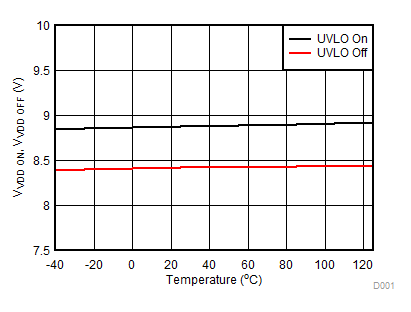
| VVDD ON | Turn-on threshold voltage of VDD | 8.0 | 8.9 | 9.8 | V | |
| VVDD OFF | Turn-off threshold voltage of VDD | 7.5 | 8.4 | 9.3 | ||
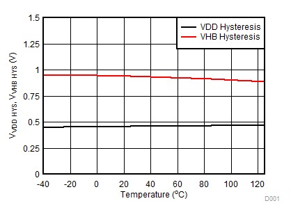
| VVDD HYS | Hysteresis of VDD | 0.5 | ||||
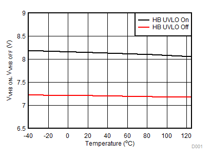
| VVHB ON | Turn-on threshold voltage of VHB–VHS | 7.2 | 8.2 | 9.2 | ||
| VVHB OFF | Turn-off threshold voltage of VHB–VHS | 6.4 | 7.3 | 8.3 | ||
| VVHB HYS | Hysteresis of VHB–VHS | 0.5 | 0.9 | |||
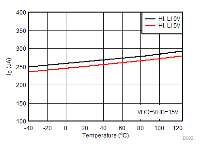
| IQ | Total quiescent supply current | HI = LI = 0 V or 5 V, DC on/off state | 180 | 255 | 420 | µA |
| IQVDD | Quiescent VDD-COM supply current | HI = LI = 0 V or 5 V, DC on/off state | 190 | 320 | ||
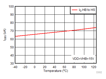
| IQBS | Quiescent HB-HS supply current | HI = 0 V or 5 V, HO in DC on/off state | 65 | 100 | ||
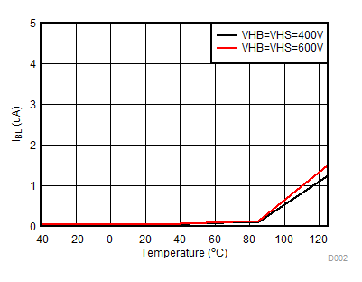
| IBL | Bootstrap supply leakage current | HB = HS = 600 V | 20 | |||
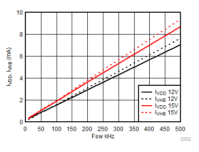
| IOP | Dynamic operating current | HI = LI = 0 V or 5 V, f = 100 kHz, duty = 50%, CL= 1 nF | 3800(1) | 4500 | ||
| INPUT BLOCK | ||||||
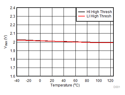
| VINH | Input Pin (HI, LI) high threshold | 1.6 | 2.0 | 2.4 | V | |
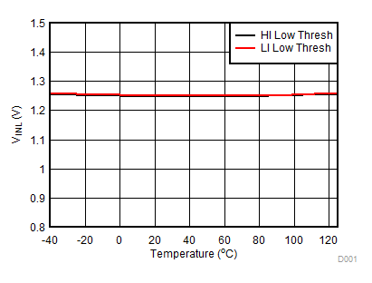
| VINL | Input Pin (HI, LI) low threshold | 0.8 | 1.2 | 1.5 | ||
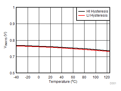
| VINHYS | Input Pin (HI, LI) threshold hysteresis | 0.8 | ||||
| IINL | HI, LI input low bias current | HI, LI = 0 V | –5 | 0 | 5 | µA |
| IINH | HI, LI input high bias current | HI, LI = 5 V | 1.7 | 70 | ||
| OUTPUT BLOCK | ||||||
| VDD-VLOH | LO output high voltage | LI = 5 V, ILO = –20 mA | 60 | 136 | mV | |
| VHB-VHOH | HO output high voltage | HI = 5 V, IHO = –20 mA | 60 | 136 | ||
| VLOL | LO output low voltage | LI = 0 V, ILO = 20 mA | 30 | 80 | ||
| VHOL | HO output low voltage | HI = 0 V, IHO = 20 mA | 30 | 80 | ||
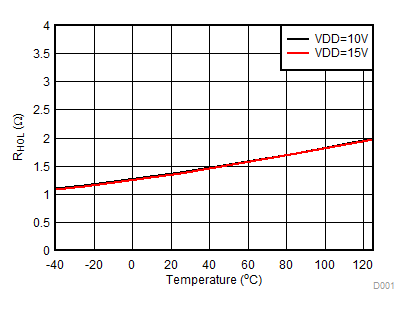
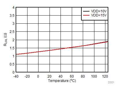
| RLOL, RHOL | LO, HO output pull-down resistance | ILO = IHO = 20 mA | 1.5 | 4 | Ω | |
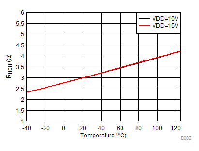
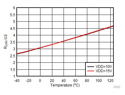
| RLOH, RHOH | LO, HO output pull-up resistance | ILO = IHO = –20 mA | 3.0 | 6.8 | ||
| IGPK-(1) | HO, LO output low short circuit pulsed current | HI = LI = 0 V, HO = LO = 15 V, PW < 10 µs | 2.8 | A | ||
| IGPK+(1) | HO, LO output high short circuit pulsed current | HI = LI = 5 V, HO = LO = 0 V, PW < 10 µs | –1.8 | |||
(1) Ensured by design, not tested in production
7.6 Dynamic Electrical Characteristics
At VDD = VHB = 15 V, COM = VHS = 0, all voltages are with respect to COM, no load on LO and HO, –40°C < TJ < +125°C (unless otherwise noted). Currents are positive into and negative out of the specified terminal.| PARAMETER | TEST CONDITIONS | MIN | NOM | MAX | UNIT | |
|---|---|---|---|---|---|---|
| DYNAMIC CHARACTERISTICS | ||||||
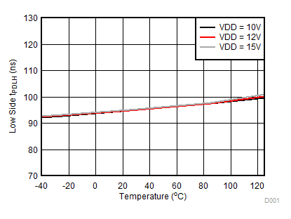
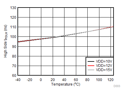
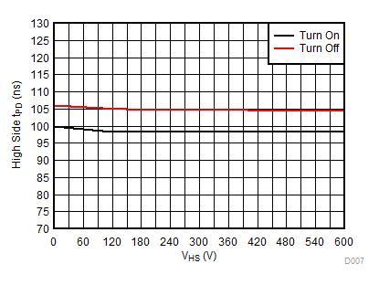
| tPDLH | Turn-on propagation delay (without deadtime) | LI to LO, HI to HO, HS = COM = 0 V | 100 | 160 | ns | |
| tPDHL | Turn-off propagation delay | LI to LO, HI to HO, HS = COM = 0 V | 100 | 160 | ||
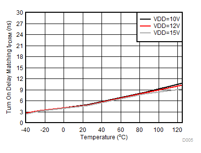
| tPDRM | Low-to-high delay matching | 5 | 30 | |||
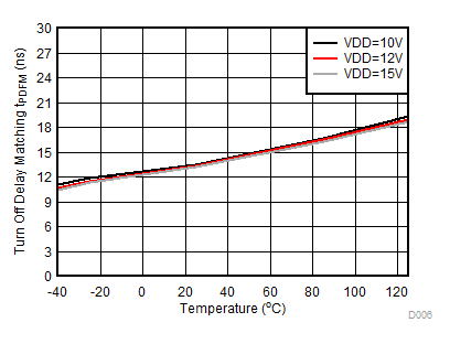
| tPDFM | High-to-low delay matching | 12 | 30 | |||
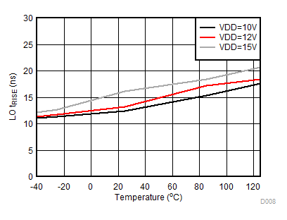
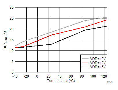
| tRISE | Turn-on rise time | 10% to 90%, HO/LO with 1000-pF load | 16 | 50 | ||
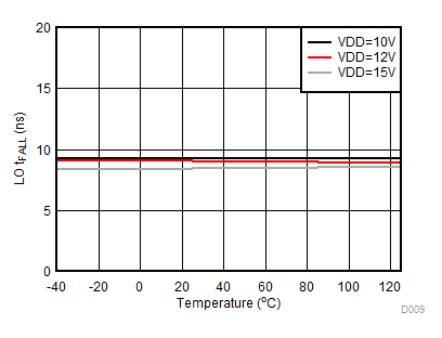
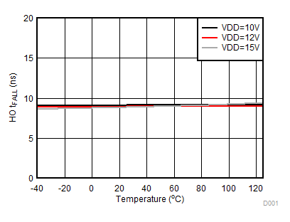
| tFALL | Turn-off fall time | 10% to 90%, HO/LO with 1000-pF load | 10 | 30 | ||
| tON | Minimum HI/LI ON pulse that changes output state | 0-V to 5-V input signal on HI and LI pins | 25 | 45 | ||
| tOFF | Minimum HI/LI OFF pulse that changes output state | 5-V to 0-V input signal on HI and LI pins | 35 | 45 | ||
| DT | Deadtime | Internal deadtime for Interlock | 100 | 150 | 200 | |
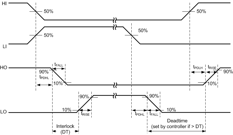 Figure 1. Typical Test Timing Diagram
7.7 Typical Characteristics
