SLUSBY6B August 2015 – March 2017 UCC27714
PRODUCTION DATA.
- 1 Features
- 2 Applications
- 3 Description
- 4 Revision History
- 5 Pin Configuration and Functions
- 6 Specifications
- 7 Detailed Description
-
8 Application and Implementation
- 8.1 Application Information
- 8.2
Typical Application
- 8.2.1 Design Requirements
- 8.2.2
Detailed Design Procedure
- 8.2.2.1 Selecting HI and LI Low Pass Filter Components (RHI, RLI, CHI, CLI)
- 8.2.2.2 Selecting Bootstrap Capacitor (CBOOT)
- 8.2.2.3 Selecting VDD Bypass/Holdup Capacitor (CVDD) and Rbias
- 8.2.2.4 Selecting Bootstrap Resistor (RBOOT)
- 8.2.2.5 Selecting Gate Resistor RHO/RLO
- 8.2.2.6 Selecting Bootstrap Diode
- 8.2.2.7 Estimate the UCC27714 Power Losses (PUCC27714)
- 8.2.2.8 Application Example Schematic Note
- 8.2.2.9 LO and HO Overshoot and Undershoot
- 8.2.3 Application Curves
- 9 Power Supply Recommendations
- 10Layout
- 11Device and Documentation Support
- 12Mechanical, Packaging, and Orderable Information
- 13Mechanical, Packaging, and Orderable Information
Package Options
Mechanical Data (Package|Pins)
- D|14
Thermal pad, mechanical data (Package|Pins)
Orderable Information
1 Features
- High-Side, Low-Side Configuration, with Independent Inputs
- Fully Operational up to 600 V (HS Pin)
- Floating Channel Designed for Bootstrap Operation
- Peak Output Current Capability of 4-A Sink 4-A Source at VDD = 15 V
- Best-In-Class Propagation Delay (125-ns Maximum)
- Best-In-Class Delay Matching (20-ns Maximum)
- TTL and CMOS Compatible Input Logic
- VDD Bias Supply Range of 10 V to 20 V
- Bias UVLO Protection for Both Channels
- Rail-to-Rail Drive
- Robust Operation Under Negative Voltage Transients
- High dv/dt Immunity (HS Pin)
- Separated Grounds for Logic (VSS) and Driver (COM) with Capability to Sustain Voltage Difference
- Optional Enable Function (Pin 4)
- Outputs Held in LOW when Inputs Floating
- Inputs and Enable Pin Voltage Levels Not Restricted by VDD Pin Bias Supply Voltage
- High and Low Voltage Pins Separated for Maximum Creepage and Clearance
- Negative Voltage Handling Capability on Input and Enable Pins
2 Applications
- Half-Bridge and Full-Bridge Converters in Offline AC and DC Power Supplies
- High-Density Switching Power Supplies for Server, Telecom, IT and Industrial Infrastructure
- Solar Inverters, Motor Drive and UPS
3 Description
UCC27714 is a 600-V high-side, low-side gate driver with 4-A source and 4-A sink current capability, targeted to drive power MOSFETs or IGBTs. The device comprises of one ground-referenced channel (LO) and one floating channel (HO) which is designed for operating with bootstrap supplies. The device features excellent robustness and noise immunity with capability to maintain operational logic at negative voltages of up to –8 VDC on HS pin (at VDD = 12 V).
The device accepts a wide range bias supply input from 10 V to 20 V and offers UVLO protection for both the VCC and HB bias supply pins. UCC27714 is available in SOIC-14 package and rated to operate from –40°C to 125°C.
Device Information(1)
| PART NUMBER | PACKAGE | BODY SIZE (NOM) |
|---|---|---|
| UCC27714 | SOIC (14) | 3.91 mm × 8.65 mm |
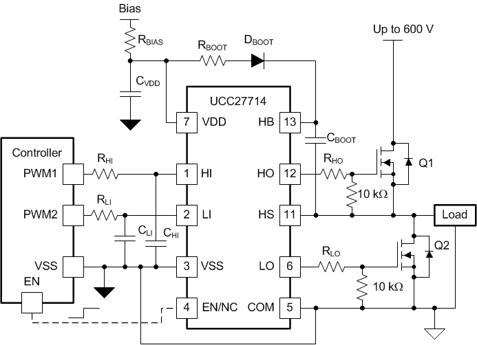
Simplified Schematic

Typical Propagation Delay Comparison
