SLUSBY6B August 2015 – March 2017 UCC27714
PRODUCTION DATA.
- 1 Features
- 2 Applications
- 3 Description
- 4 Revision History
- 5 Pin Configuration and Functions
- 6 Specifications
- 7 Detailed Description
-
8 Application and Implementation
- 8.1 Application Information
- 8.2
Typical Application
- 8.2.1 Design Requirements
- 8.2.2
Detailed Design Procedure
- 8.2.2.1 Selecting HI and LI Low Pass Filter Components (RHI, RLI, CHI, CLI)
- 8.2.2.2 Selecting Bootstrap Capacitor (CBOOT)
- 8.2.2.3 Selecting VDD Bypass/Holdup Capacitor (CVDD) and Rbias
- 8.2.2.4 Selecting Bootstrap Resistor (RBOOT)
- 8.2.2.5 Selecting Gate Resistor RHO/RLO
- 8.2.2.6 Selecting Bootstrap Diode
- 8.2.2.7 Estimate the UCC27714 Power Losses (PUCC27714)
- 8.2.2.8 Application Example Schematic Note
- 8.2.2.9 LO and HO Overshoot and Undershoot
- 8.2.3 Application Curves
- 9 Power Supply Recommendations
- 10Layout
- 11Device and Documentation Support
- 12Mechanical, Packaging, and Orderable Information
- 13Mechanical, Packaging, and Orderable Information
Package Options
Mechanical Data (Package|Pins)
- D|14
Thermal pad, mechanical data (Package|Pins)
Orderable Information
8 Application and Implementation
NOTE
Information in the following Applications section is not part of the TI component specification, and TI does not warrant its accuracy or completeness. TI’s customers are responsible for determining suitability of components for their purposes. Customers should validate and test their design implementation to confirm system functionality.
8.1 Application Information
To effect fast switching of power devices and reduce associated switching power losses, a powerful gate driver is employed between the PWM output of controllers and the gates of the power semiconductor devices. Also, gate drivers are indispensable when it is impossible for the PWM controller to directly drive the gates of the switching devices. With the advent of digital power, this situation will be often encountered because the PWM signal from the digital controller is often a 3.3-V logic signal which cannot effectively turn on a power switch. Level shifting circuitry is needed to boost the 3.3-V signal to the gate-drive voltage (such as 12 V) in order to fully turn on the power device and minimize conduction losses. Traditional buffer drive circuits based on NPN/PNP bipolar transistors in totem-pole arrangement, being emitter follower configurations, prove inadequate with digital power because they lack level-shifting capability.
Gate drivers effectively combine both the level-shifting and buffer-drive functions. Gate drivers also find other needs such as minimizing the effect of high-frequency switching noise by locating the high-current driver physically close to the power switch, driving gate-drive transformers and controlling floating power-device gates, reducing power dissipation and thermal stress in controllers by moving gate charge power losses from the controller into the driver.
8.2 Typical Application
The circuit in Figure 54 shows two UCC27714 in a phase shifted full bridge setup converting 370 V – 410 V DC into 12 V while driving up to 50-A output current. The UCC27524A drives the secondary side. All gate drivers are controlled by the UCC28950. The leading leg is shown in detail.
For more information, please refer to UCC27714EVM-551.
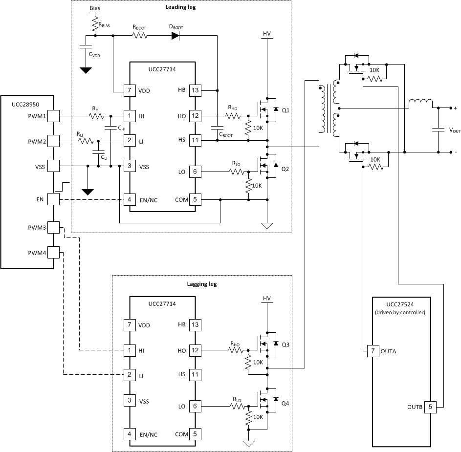 Figure 54. Typical Application Schematic
8.2.1 Design Requirements
Table 4 shows the design requirements for a 600-W power supply used as an example to illustrate the design process.
Table 4. UCC27714 Design Requirements
| PARAMETER | TEST CONDITIONS | MIN | TYP | MAX | UNIT | |
|---|---|---|---|---|---|---|
| INPUT CHARACTERISTICS | ||||||
| DC input voltage range | 370 | 390 | 410 | V | ||
| IIN(max) | Maximum input current | VIN= 370 VDC to 410 VDC | 2 | A | ||
| OUTPUT CHARACTERISTICS | ||||||
| VOUT | Output voltage | VIN = 370 VDC to 410 VDC | 11.4 | 12 | 12.6 | V |
| IOUT | Output current | VIN = 370 VDC to 410 VDC | 50 | A | ||
| POUT | Continuous output power | VIN = 370 VDC to 410 VDC | 600 | W | ||
8.2.2 Detailed Design Procedure
This procedure outlines the steps to design a 600-V high-side, low-side gate driver with 4-A source and 4-A sink current capability, targeted to drive power MOSFETs or IGBTs using the UCC27714. Refer to Figure 54 for component names and network locations. For additional design help see the UCC27714EVM-551 User Guide, SLUUB02.
8.2.2.1 Selecting HI and LI Low Pass Filter Components (RHI, RLI, CHI, CLI)
A RC filter should be added between PWM controller and input pin of UCC27714 to filter the high frequency noise, like RHI/CHI and RLI/CLI which shown in Figure 54. The recommended values of the RC filter is refer to Equation 1 and Equation 2:


8.2.2.2 Selecting Bootstrap Capacitor (CBOOT)
The bootstrap capacitor should be sized to have more than enough energy to drive the gate of FET Q1 high, without depleting the boot capacitor more than 10%. A good rule of thumb is size CBOOT to be at least 10 times; as large as the equivalent FET gate capacitance (Cg).
Cg will have to be calculated based voltage driving the high side FET’s gate (VQ1g ) and knowing the FET’s gate charge (Qg). VQ1g is approximately the bias voltage supplied to VDD less the forward voltage drop of the boost diode (VDBOOT). In this design example, the estimated VQ1g was approximately 11.4V

The FET used in this example had a specified Qg of 87 nC. Based on Qg and VQ1g the calculated Cg was 7.63 nF.
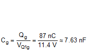
Once Cg is estimated CBOOT should be sized to be at least 10 times larger than Cg.

For this design example a 100-nF capacitor was chosen for the bootstrap capacitor.

8.2.2.3 Selecting VDD Bypass/Holdup Capacitor (CVDD) and Rbias
The VDD capacitor (CVDD) should be chosen to be at least 10 times larger than CBOOT. For this design example a 1-µF capacitor was selected.

A 5-Ω resistor RBIAS in series with bias supply and VDD pin is recommended to make the VDD ramp up time larger than 50 µs to prevent error logic error spikes on the outputs as shown in Figure 55
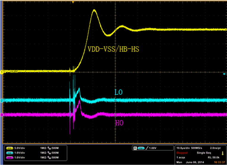 Figure 55. VDD/HB-HS Fast Ramp Up
8.2.2.4 Selecting Bootstrap Resistor (RBOOT)
Resistor RBOOT is selected to limit the current in DBOOT and limit the ramp up slew rate of voltage of HB-HS to avoid the phenomenon shown in Figure 55. It is recommended when using the UCC27714 that RBOOT is between 2 Ω and 10 Ω. For this design we selected a current limiting resistor of 2.2 Ω. The bootstrap diode current (IDBOOT(pk)) was limited to roughly 5.2 A.


The power dissipation capability of the bootstrap resistor is important. The bootstrap resistor must be able to withstand the short period of high power dissipation during the initial charging sequence of the boot-strap capacitor. This energy is equivalent to 1/2 × CBOOT × V2. This energy is dissipated during the charging time of the bootstrap capacitor (~3 × RBOOT × CBOOT). Special attention must be paid to use a bigger size RBOOT when a bigger value of CBOOT is chosen.
8.2.2.5 Selecting Gate Resistor RHO/RLO
Resistor RHO and RLO are sized to reduce ringing caused by parasitic inductances and capacitances and also to limit the current coming out of the gate driver. For this design 3.01-Ω resistors were selected for this design.

Maximum HO Drive Current (IHO_DR):

Maximum HO Sink Current (IHO_SK):

Maximum LO Drive Current (ILO_DR):

Maximum LO Sink Current (ILO_SK):

In applications with high dV/dt switching and/or significant ringing on the HS node, the HO output may exhibit a short duration pulse although the HI input is high for a longer time. MOSFET’s with slow body diode recovery time can result in high dV/dt transitions and excessive ringing in hard switching conditions. If the user observes this condition the problem can be corrected by increasing RHO and RLO to limit HS dV/dt and ringing to <50 V/ns dVHS/dt specification of the UCC27714. Refer to Figure 56 below.
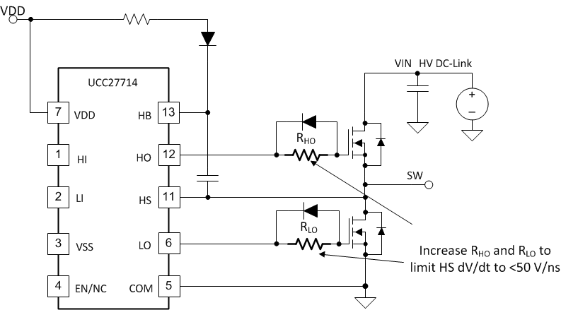 Figure 56. Increase RHO and RLO, Reduce HS dV/dt
8.2.2.6 Selecting Bootstrap Diode
A fast recovery diode should be chosen to avoid charge is taken away from the bootstrap capacitor. Thus, a fast reverse recovery time tRR, low forward voltage VF and low junction capacitance is recommended.
Suggested parts include MURA160T3G and BYG20J.
8.2.2.7 Estimate the UCC27714 Power Losses (PUCC27714)
The power losses of UCC27714 (PUCC27714) are estimated by calculating losses from several components:
The static power losses due to quiescent current (IQDD, IQBS) are calculated in Equation 15:

Static losses due to leakage current (IBL) are calculated from the HB high-voltage node as shown in Equation 16:

Dynamic losses incurred due to the gate charge while driving the FETs Q1 and Q2 are calculated Equation 17. Please note that this component typically dominates over the dynamic losses related to the internal VDD & VHB switching logic circuitry in UCC27714.

Equation 18 calculates dynamic losses during the operation of the level shifter at HO turn-off edge. QP, typically 0.5 nC, is the charge absorbed by the level shifter during operation at each edge. Please note that if high-voltage switching occurs during HO turn-on as well (as in the case of ZVS topologies), then the power loss due to this component must be effectively doubled.

The total power losses are calculated in Equation 19:

For the conditions, VDD=VBS=15V, VHB = VHS + VBS = 400V, HO On-state Duty cycle D = 50%, QG = 87nC, fSW = 100kHz, the total power loss in UCC27714 driver for a ZVS power supply topology can be estimated as follows, assuming no external gate drive resistors are used in the design:

When external resistors are used in the gate drive circuit, a portion of this power loss is incurred on these external resistors and the power loss in UCC27714 will be lower, allowing the device to run at lower temperatures.
8.2.2.8 Application Example Schematic Note
In the application example schematic there are 10-kΩ resistors across the gate and source terminals of FET Q1 and Q2. These resistors are placed across these nodes to ensure FETs Q1 and Q2 are not turned on if the UCC27714 is not in place or properly soldered to the circuit board or if UCC27714 is in an unbiased state.
8.2.2.9 LO and HO Overshoot and Undershoot
The LO and HO driver outputs may exhibit output overshoot beyond the VDD or HB level or output undershoot below COM or HS. This overshoot and/or undershoot is typically due to the high di/dt during switch transition and parasitic inductance, including PC board trace inductance and device package inductance in the driver gate drive current loop. If the driver output overshoot or undershoot exceeds the datasheet limits of –0.3 V DC, –2 V for 100 ns, or VDD (VHB) +0.3 V, the driver output can be in the incorrect state. If the user observes the incorrect output behavior, the issue can be resolved by slowing down the di/dt and dv/dt by increasing the gate drive resistance, see Figure 56, or adding Schottky diodes to the HO and LO outputs to clamp the driver LO output to VDD and COM, and the HO output to HB and HS. Refer to Figure 57 below for diode placement. The diodes must be placed close to the IC pins and connected with short traces.
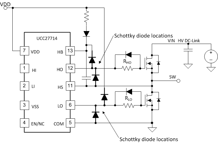 Figure 57. Driver Overshoot and Undershoot Clamp Diodes
8.2.3 Application Curves
Figure 58 and Figure 59 show the measured LI to LO turn-on and turn-off delay of one UCC27714 device. Channel 1 depicts VDD, Channel 2 LO and Channel 3 LI.
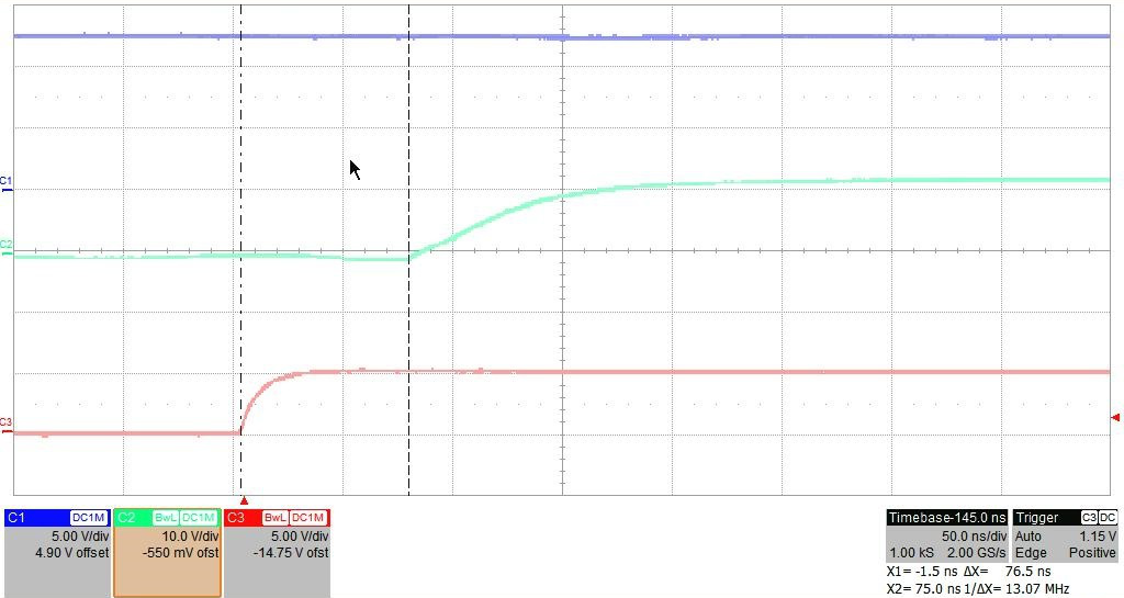 Figure 58. LI to LO Turn-On Propagation Delay
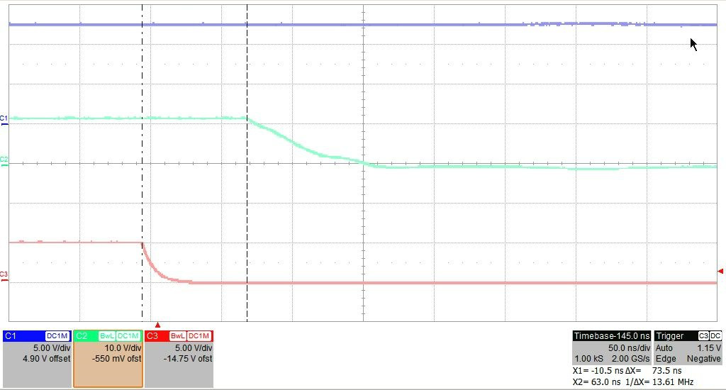 Figure 59. LI to LO Turn-Off Propagation Delay
Figure 60 and Figure 61 show the measured HI to HO turn-on and turn-off delay of one UCC27714 device. Channel 1 depicts HI, Channel 2 LO, Channel 3 HO and Channel 4 VDD.
NOTE
HO was measured with a 1:20 differential probe.
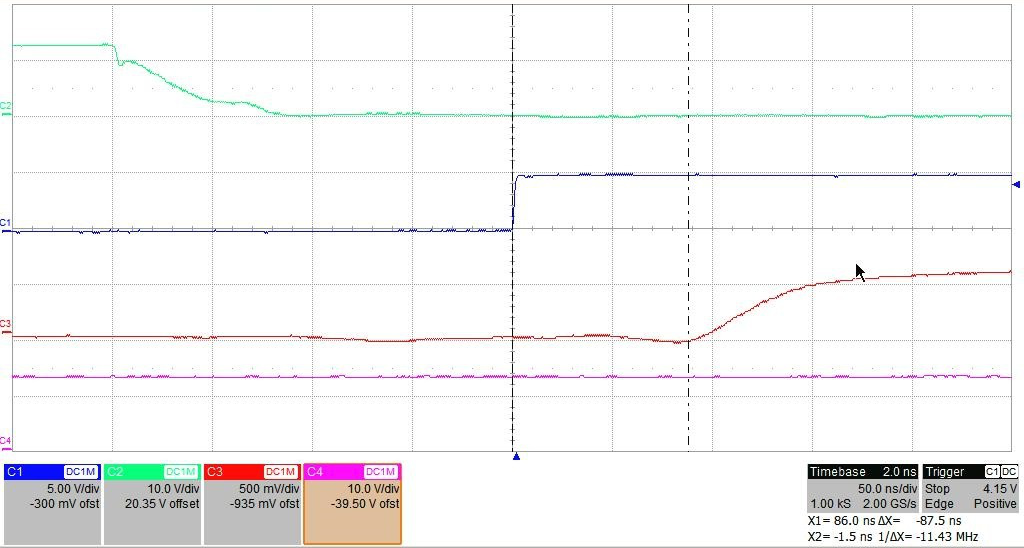 Figure 60. HI to HO Turn-On Propagation Delay
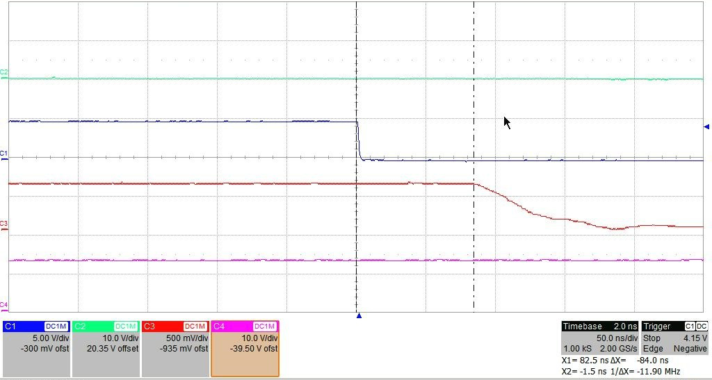 Figure 61. HI to HO Turn-Off Propagation Delay