SNVSA88C December 2014 – November 2016 UCC28063A
PRODUCTION DATA.
- 1 Features
- 2 Applications
- 3 Description
- 4 Revision History
- 5 Description (Continued)
- 6 Pin Configuration and Functions
- 7 Specifications
-
8 Detailed Description
- 8.1 Overview
- 8.2 Functional Block Diagram
- 8.3
Feature Description
- 8.3.1 Principles of Operation
- 8.3.2 Natural Interleaving
- 8.3.3 On-Time Control, Maximum Frequency Limiting, and Restart Timer
- 8.3.4 Distortion Reduction
- 8.3.5 Zero-Current Detection and Valley Switching
- 8.3.6 Phase Management and Light-Load Operation
- 8.3.7 External Disable
- 8.3.8 Improved Error Amplifier
- 8.3.9 Soft Start
- 8.3.10 Brownout Protection
- 8.3.11 Dropout Detection
- 8.3.12 VREF
- 8.3.13 VCC
- 8.3.14 Control of Downstream Converter
- 8.3.15
System Level Protections
- 8.3.15.1 Failsafe OVP - Output Overvoltage Protection
- 8.3.15.2 Overcurrent Protection
- 8.3.15.3 Open-Loop Protection
- 8.3.15.4 VCC Undervoltage Lock-Out (UVLO) Protection
- 8.3.15.5 Phase-Fail Protection
- 8.3.15.6 Thermal Shutdown Protection
- 8.3.15.7 AC-Line Brownout and Dropout Protections
- 8.3.15.8 Fault Logic Diagram
- 8.4 Device Functional Modes
-
9 Applications and Implementation
- 9.1 Application Information
- 9.2
Typical Application
- 9.2.1 Design Requirements
- 9.2.2
Detailed Design Procedure
- 9.2.2.1 Inductor Selection
- 9.2.2.2 ZCD Resistor Selection (RZA, RZB)
- 9.2.2.3 HVSEN
- 9.2.2.4 Output Capacitor Selection
- 9.2.2.5 Selecting (RS) For Peak Current Limiting
- 9.2.2.6 Power Semiconductor Selection (Q1, Q2, D1, D2)
- 9.2.2.7 Brownout Protection
- 9.2.2.8 Converter Timing
- 9.2.2.9 Programming VOUT
- 9.2.2.10 Voltage Loop Compensation
- 9.2.3 Application Curves
- 10Power Supply Recommendations
- 11Layout
- 12Device and Documentation Support
- 13Mechanical, Packaging, and Orderable Information
Package Options
Mechanical Data (Package|Pins)
- D|16
Thermal pad, mechanical data (Package|Pins)
Orderable Information
11 Layout
11.1 Layout Guidelines
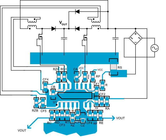
Interleaved transition-mode PFC system architecture dramatically reduces input and output ripple current, allowing the circuit to use smaller and less expensive filters. To maximize the benefits of interleaving, the input and output filter capacitors should be located after the two phase currents are combined together. Similar to other power management devices, when laying out the printed circuit board (PCB) it is important to use star grounding techniques and keep filter capacitors as close to device ground as possible. To minimize the interference caused by capacitive coupling from the boost inductor, the device should be located at least 1 in (25.4 mm) away from the boost inductor. It is also recommended that the device not be placed underneath magnetic elements. Because of the precise timing requirement, timing-setting resistor RT should be placed as close as possible to the TSET pin and returned to the analog ground pin with the shortest possible path. See Figure 39 for a recommended component placement and layout.
11.2 Layout Example
