SLUSAW0B March 2012 – December 2023 UCC28070A
PRODUCTION DATA
- 1
- 1 Features
- 2 Applications
- 3 Description
- 4 Pin Configuration and Functions
- 5 Specifications
-
6 Detailed Description
- 6.1 Overview
- 6.2 Functional Block Diagram
- 6.3
Feature Description
- 6.3.1 Interleaving
- 6.3.2 Programming the PWM Frequency and Maximum Duty-Cycle Clamp
- 6.3.3 Frequency Dithering (Magnitude and Rate)
- 6.3.4 External Clock Synchronization
- 6.3.5 Multi-phase Operation
- 6.3.6 VSENSE and VINAC Resistor Configuration
- 6.3.7 VSENSE and VINAC Open-Circuit Protection
- 6.3.8 Current Synthesizer
- 6.3.9 Programmable Peak Current Limit
- 6.3.10 Linear Multiplier and Quantized Voltage Feed Forward
- 6.3.11 Enhanced Transient Response (VA Slew-Rate Correction)
- 6.3.12 Voltage Biasing (VCC and VVREF)
- 6.3.13 PFC Enable and Disable
- 6.3.14 Adaptive Soft Start
- 6.3.15 PFC Start-Up Hold Off
- 6.3.16 Output Overvoltage Protection (OVP)
- 6.3.17 Zero-Power Detection
- 6.3.18 Thermal Shutdown
- 6.3.19 Current Loop Compensation
- 6.3.20 Voltage Loop Compensation
- 6.4 Device Functional Modes
-
7 Application and Implementation
- 7.1 Application Information
- 7.2
Typical Application
- 7.2.1 Design Requirements
- 7.2.2
Detailed Design Procedure
- 7.2.2.1 Output Current Calculation
- 7.2.2.2 Bridge Rectifier
- 7.2.2.3 PFC Inductor (L1 and L2)
- 7.2.2.4 PFC MOSFETs (M1 and M2)
- 7.2.2.5 PFC Diode
- 7.2.2.6 PFC Output Capacitor
- 7.2.2.7 Current-Loop Feedback Configuration (Sizing of the Current-Transformer Turns-Ratio and Sense Resistor (RS))
- 7.2.2.8 Current-Sense Offset and PWM Ramp for Improved Noise Immunity
- 7.2.3 Application Curves
- 7.3 Power Supply Recommendations
- 7.4 Layout
- 8 Device and Documentation Support
- 9 Revision History
- 10Mechanical, Packaging, and Orderable Information
Package Options
Mechanical Data (Package|Pins)
- PW|20
Thermal pad, mechanical data (Package|Pins)
- PW|20
Orderable Information
6.3.20 Voltage Loop Compensation
The outer voltage control loop of the dual-phase PFC controller functions the same as with a single-phase controller, and compensation techniques for loop stability are standard [7]. The bandwidth of the voltage-loop must be considerably lower than the twice-line ripple frequency (f2LF) on the output capacitor to avoid distortion-causing correction to the output voltage. The output of the voltage-error amplifier (VVAO) is an input to the multiplier to adjust the input current amplitude relative to the required output power. Variations on VAO within the bandwidth of the current loops influences the wave-shape of the input current. Because the low-frequency ripple on COUT is a function of input power only, its peak-to-peak amplitude is the same at high-line as at low-line. Any response of the voltage-loop to this ripple has a greater distorting effect on high-line current than on low-line current. Therefore, the allowable percentage of 3rd-harmonic distortion on the input current contributed by VAO must be determined using high-line conditions.
Because the voltage-error amplifier (VA) is a transconductance type of amplifier, the impedance on its input has no bearing on the amplifier gain, which is determined solely by the product of its transconductance (gmv) with its output impedance (ZOV). Thus, the VSENSE input divider-network values are determined separately based on criteria discussed in VSENSE and VINAC Open-Circuit Protection. Its output is the VAO pin.
 Figure 6-6 Voltage
Error Amplifier With Type II Compensation
Figure 6-6 Voltage
Error Amplifier With Type II CompensationThe twice-line ripple voltage component of VVSENSE must be sufficiently attenuated and phase-shifted at VAO to achieve the desired level of 3rd-harmonic distortion of the input current wave-shape [4]. For every 1% of 3rd-harmonic input distortion allowable, the small-signal gain GVEA = VVAOpk / vSENSEpk = gmv × ZOV at the twice-line frequency must allow no more than 2% ripple over the full VVAO voltage range. In the UCC28070A, VVAO can range from 1V at zero load power to approximately 4.2V at full load power for a ΔVVAO = 3.2V, so 2% of 3.2V is 64mV peak ripple.
Although the maximum VVAO is clamped at 5V, at full load VVAO may vary around an approximate center point of 4.2V to compensate for the effects of the quantized feed-forward voltage in the multiplier stage (see Linear Multiplier and Quantized Voltage Feed Forward for details). Therefore, 4.2V is the proper voltage to use to represent maximum output power when performing voltage-loop gain calculations.
The output capacitor maximum low-frequency, zero-to-peak, ripple voltage is closely approximated by:
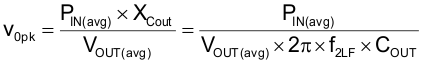
where:
- PIN(avg) is the total maximum input power of the interleaved-PFC preregulator
- VOUT(avg) is the average output voltage
- COUT is the output capacitance
where
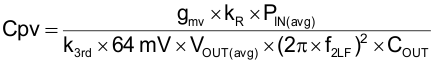
- kR is the gain of the resistor-divider network on VSENSE
Thus, for k3rd, the percentage of allowable 3rd-harmonic distortion on the input current attributable to the VAO ripple,
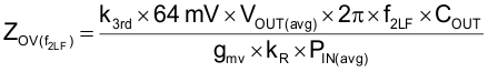
This impedance on VAO is set by a capacitor (CPV), where CPV = 1 / (2πf2LF × ZOV(f2LF)); therefore:
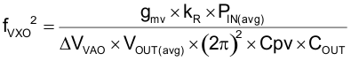
The voltage-loop unity-gain cross-over frequency (fVXO) may now be solved by setting the open-loop voltage transfer function gain equal to 1:
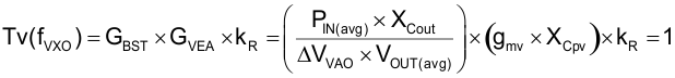
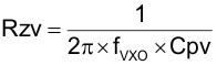
The zero-resistor (RZV) from the zero-placement network of the compensation may now be calculated. Together with CPV, RZV sets a pole right at fVXO to obtain 45° phase margin at the cross-over.
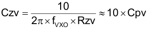
Finally, a zero is placed at or below fVXO / 6 with capacitor CZV to provide high gain at DC but with a breakpoint far enough below fVXO so as not to significantly reduce the phase margin. Choosing fVXO / 10 allows one to approximate the parallel combination value of CZV and CPV as CZV, and solve for CZV simply as:
By using a spreadsheet or math program, CZV, RZV, and CPV may be manipulated to observe their effects on fVXO and phase margin and the percentage contribution to 3rd-harmonic distortion. Also, phase margin may be checked as PIN(avg) level and system parameter tolerances vary.
The percentage of 3rd-harmonic distortion calculated in this section represents the contribution from the f2LF voltage ripple on COUT only. Other sources of distortion, such as the current-sense transformer, the current synthesizer stage, excessively-limited DMAX, and so on, can contribute additional 3rd and higher-order harmonic distortion.