SLUSAW0C March 2012 – July 2025 UCC28070 , UCC28070A
PRODUCTION DATA
- 1
- 1 Features
- 2 Applications
- 3 Description
- 4 Pin Configuration and Functions
- 5 Specifications
-
6 Detailed Description
- 6.1 Overview
- 6.2 Functional Block Diagram
- 6.3
Feature Description
- 6.3.1 Interleaving
- 6.3.2 Programming the PWM Frequency and Maximum Duty-Cycle Clamp
- 6.3.3 Frequency Dithering (Magnitude and Rate)
- 6.3.4 External Clock Synchronization
- 6.3.5 Multi-phase Operation
- 6.3.6 VSENSE and VINAC Resistor Configuration
- 6.3.7 VSENSE and VINAC Open-Circuit Protection
- 6.3.8 Current Synthesizer
- 6.3.9 Programmable Peak Current Limit
- 6.3.10 Linear Multiplier and Quantized Voltage Feed Forward
- 6.3.11 Enhanced Transient Response (VA Slew-Rate Correction)
- 6.3.12 Bias Voltages (VCC and VREF)
- 6.3.13 PFC Enable and Disable
- 6.3.14 Adaptive Soft-Start
- 6.3.15 PFC Start-Up Hold Off
- 6.3.16 Output Overvoltage Protection (OVP)
- 6.3.17 Zero-Power Detection
- 6.3.18 Thermal Shutdown
- 6.3.19 Current Loop Compensation
- 6.3.20 Voltage Loop Compensation
- 6.4 Device Functional Modes
-
7 Application and Implementation
- 7.1 Application Information
- 7.2
Typical Application
- 7.2.1 Design Requirements
- 7.2.2
Detailed Design Procedure
- 7.2.2.1 Output Current Calculation
- 7.2.2.2 Bridge Rectifier
- 7.2.2.3 PFC Inductor (L1 and L2)
- 7.2.2.4 PFC MOSFETs (M1 and M2)
- 7.2.2.5 PFC Diode
- 7.2.2.6 PFC Output Capacitor
- 7.2.2.7 Current-Loop Feedback Configuration (Sizing of the Current-Transformer Turns-Ratio NCT and Current-Sense Resistor RS)
- 7.2.2.8 Current-Sense Offset and PWM Ramp for Improved Noise Immunity
- 7.2.3 Application Curves
- 7.3 Power Supply Recommendations
- 7.4 Layout
- 8 Device and Documentation Support
- 9 Revision History
- 10Mechanical, Packaging, and Orderable Information
Package Options
Mechanical Data (Package|Pins)
- PW|20
Thermal pad, mechanical data (Package|Pins)
Orderable Information
7.2.2.2 Bridge Rectifier
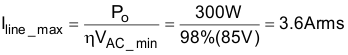
The maximum RMS input-line current is given by Equation 37:
The peak input current is given by Equation 38:

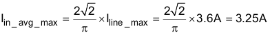
The maximum average rectified line current is given by Equation 39:
A typical bridge rectifier has a forward voltage drop VF of 0.95V at Iin_pk. The maximum power loss in the rectifier bridge can be conservatively estimated by Equation 40:

The bridge rectifier must be rated to carry the full line current plus any anticipated line-surge peaks. The bridge rectifier also carries the full inrush current as the bulk capacitor COUT charges when the line is connected. The voltage rating of the bridge is recommended to maintain suitable margin to the maximum anticipated peak input voltage including AC-line swells.