SLUSAW0B March 2012 – December 2023 UCC28070A
PRODUCTION DATA
- 1
- 1 Features
- 2 Applications
- 3 Description
- 4 Pin Configuration and Functions
- 5 Specifications
-
6 Detailed Description
- 6.1 Overview
- 6.2 Functional Block Diagram
- 6.3
Feature Description
- 6.3.1 Interleaving
- 6.3.2 Programming the PWM Frequency and Maximum Duty-Cycle Clamp
- 6.3.3 Frequency Dithering (Magnitude and Rate)
- 6.3.4 External Clock Synchronization
- 6.3.5 Multi-phase Operation
- 6.3.6 VSENSE and VINAC Resistor Configuration
- 6.3.7 VSENSE and VINAC Open-Circuit Protection
- 6.3.8 Current Synthesizer
- 6.3.9 Programmable Peak Current Limit
- 6.3.10 Linear Multiplier and Quantized Voltage Feed Forward
- 6.3.11 Enhanced Transient Response (VA Slew-Rate Correction)
- 6.3.12 Voltage Biasing (VCC and VVREF)
- 6.3.13 PFC Enable and Disable
- 6.3.14 Adaptive Soft Start
- 6.3.15 PFC Start-Up Hold Off
- 6.3.16 Output Overvoltage Protection (OVP)
- 6.3.17 Zero-Power Detection
- 6.3.18 Thermal Shutdown
- 6.3.19 Current Loop Compensation
- 6.3.20 Voltage Loop Compensation
- 6.4 Device Functional Modes
-
7 Application and Implementation
- 7.1 Application Information
- 7.2
Typical Application
- 7.2.1 Design Requirements
- 7.2.2
Detailed Design Procedure
- 7.2.2.1 Output Current Calculation
- 7.2.2.2 Bridge Rectifier
- 7.2.2.3 PFC Inductor (L1 and L2)
- 7.2.2.4 PFC MOSFETs (M1 and M2)
- 7.2.2.5 PFC Diode
- 7.2.2.6 PFC Output Capacitor
- 7.2.2.7 Current-Loop Feedback Configuration (Sizing of the Current-Transformer Turns-Ratio and Sense Resistor (RS))
- 7.2.2.8 Current-Sense Offset and PWM Ramp for Improved Noise Immunity
- 7.2.3 Application Curves
- 7.3 Power Supply Recommendations
- 7.4 Layout
- 8 Device and Documentation Support
- 9 Revision History
- 10Mechanical, Packaging, and Orderable Information
Package Options
Mechanical Data (Package|Pins)
- PW|20
Thermal pad, mechanical data (Package|Pins)
- PW|20
Orderable Information
6.3.8 Current Synthesizer
One of the most prominent innovations in the UCC28070A design is the current synthesizer circuitry that synchronously monitors the instantaneous inductor current through a combination of ON-time sampling and OFF-time down-slope emulation.
During the ON-time of the GDA and GDB outputs, the inductor current is recorded at the CSA and CSB pins, respectively, through the current transformer network in each output phase. Meanwhile, the continuous monitoring of the input and output voltages through the VINAC and VSENSE pins permits the UCC28070A to internally recreate the down-slope of the inductor current during the respective OFF-time of each output. Through the selection of the RSYNTH resistor (RSYN), based on Equation 12, the internal response may be adjusted to accommodate the wide range of inductances expected across the wide array of applications.
During inrush surge events at power up and AC drop-out recovery, VVSENSE < VVINAC, the synthesized downslope becomes zero. In this case, the synthesized inductor current remains above the IMO reference and the current loop drives the duty cycle to zero. This avoids excessive stress on the MOSFETs during the surge event. Once VVINAC falls below VVSENSE, the duty cycle increases until steady-state operation resumes.
 Figure 6-2 Downslope
of the Inductor Current
Figure 6-2 Downslope
of the Inductor Current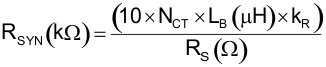
where:
- LB = Nominal Zero-Bias Boost Inductance (μH)
- RS = Sense Resistor (Ω)
- NCT = Current-sense Transformer turns ratio
- kR = RB / (RA + RB) = the resistor-divider attenuation at the VSENSE and VINAC pins