SLUSBQ5D November 2013 – July 2016 UCC28180
PRODUCTION DATA.
- 1 Features
- 2 Applications
- 3 Description
- 4 Revision History
- 5 Description (Continued)
- 6 Pin Configuration and Functions
- 7 Specifications
-
8 Detailed Description
- 8.1 Overview
- 8.2 Functional Block Diagram
- 8.3
Feature Description
- 8.3.1 Soft Start
- 8.3.2 System Protection
- 8.3.3 VCC Undervoltage LockOut (UVLO)
- 8.3.4 Output Overvoltage Protection (OVP)
- 8.3.5 Open Loop Protection/Standby (OLP/Standby)
- 8.3.6 ISENSE Open-Pin Protection (ISOP)
- 8.3.7 ICOMP Open-Pin Protection (ICOMPP)
- 8.3.8 FAULT Protection
- 8.3.9 Output Overvoltage Detection (OVD), Undervoltage Detection (UVD) and Enhanced Dynamic Response (EDR)
- 8.3.10 Overcurrent Protection
- 8.3.11 Soft Overcurrent (SOC)
- 8.3.12 Peak Current Limit (PCL)
- 8.3.13 Current Sense Resistor, RISENSE
- 8.3.14 ISENSE Pin
- 8.3.15 Gate Driver
- 8.3.16 Current Loop
- 8.3.17 ISENSE and ICOMP Functions
- 8.3.18 Pulse Width Modulator
- 8.3.19 Control Logic
- 8.3.20 Voltage Loop
- 8.3.21 Output Sensing
- 8.3.22 Voltage Error Amplifier
- 8.3.23 Non-Linear Gain Generation
- 8.4 Device Functional Modes
-
9 Application and Implementation
- 9.1 Application Information
- 9.2
Typical Application
- 9.2.1 Design Requirements
- 9.2.2
Detailed Design Procedure
- 9.2.2.1 Current Calculations
- 9.2.2.2 Switching Frequency
- 9.2.2.3 Bridge Rectifier
- 9.2.2.4 Inductor Ripple Current
- 9.2.2.5 Input Capacitor
- 9.2.2.6 Boost Inductor
- 9.2.2.7 Boost Diode
- 9.2.2.8 Switching Element
- 9.2.2.9 Sense Resistor
- 9.2.2.10 Output Capacitor
- 9.2.2.11 Output Voltage Set Point
- 9.2.2.12 Loop Compensation
- 9.2.3 Application Curve
- 10Power Supply Recommendations
- 11Layout
- 12Device and Documentation Support . .
- 13Mechanical, Packaging, and Orderable Information
Package Options
Mechanical Data (Package|Pins)
- D|8
Thermal pad, mechanical data (Package|Pins)
Orderable Information
8 Detailed Description
8.1 Overview
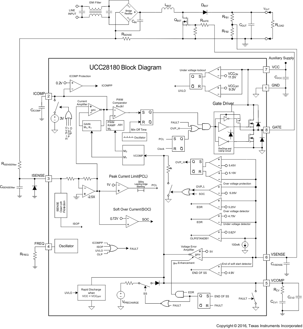
The UCC28180 is a boost controller for power factor correction operating at a fixed frequency in continuous conduction mode. The UCC28180 requires few external components to operate as an active PFC pre-regulator.
UCC28180 employs two control loops. An internal error amplifier and 5-V reference provide a slow outer loop to control output voltage. External compensation of this outer loop is applied by means of the VCOMP pin. The inner current loop shapes the average input current to match the sinusoidal input voltage. The inner current loop avoids the need to sense input voltage by exploiting the relationship between input voltage and boost duty-cycle. External compensation of the inner current loop is applied by means of the ICOMP pin.
The operating switching frequency can be programmed from 18 kHz to 250 kHz simply by connecting the FREQ pin to ground through a resistor.
UCC28180 includes a number of protection functions designed to ensure it is reliable, and will provide safe operation under all conditions, including abnormal or fault conditions.
8.3 Feature Description
8.3.1 Soft Start
Soft-Start controls the rate of rise of VCOMP in order to obtain a linear control of the increasing duty cycle as a function of time. VCOMP, the output of the voltage loop transconductance amplifier, is pulled low during UVLO, ICOMPP, ISOP and OLP (Open-Loop Protection)/STANDBY. Once the fault condition is released, an initial pre-charge source rapidly charges VCOMP to 1.5 V. After that point, a constant 40 µA of current is sourced into the compensation components causing the voltage on this pin to ramp linearly until the output voltage reaches 85% of its final value. At this point, the sourcing current decreases until the output voltage reaches its final rated voltage. The soft-start time is controlled by the voltage error amplifier compensation capacitor values selected, and is user programmable based on desired loop crossover frequency. Once the output voltage exceeds 98% of rated voltage, soft start is over, the initial pre-charge source is disconnected, and EDR is no longer inhibited.
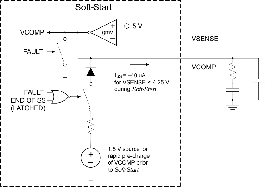 Figure 23. Soft Start
8.3.2 System Protection
System-level protection features help keep the system within safe operating limits.
8.3.3 VCC Undervoltage LockOut (UVLO)
 Figure 24. UVLO
During startup, Under-Voltage LockOut (UVLO) keeps the device in the off state until VCC rises above the 11.5-V enable threshold, VCCON. With a typical 1.7 V of hysteresis on UVLO to increase noise immunity, the device turns off when VCC drops to the 9.5-V disable threshold, VCCOFF.
If, during a brief AC-line dropout, the VCC voltage falls below the level necessary to bias the internal FAULT circuitry, the UVLO condition enables a special rapid discharge circuit which continues to discharge the VCOMP capacitors through a low impedance despite a complete lack of VCC. This helps to avoid an excessive current surge should the AC-line return while there is still substantial voltage stored on the VCOMP capacitors. Typically, these capacitors can be discharged to less than 1 V within 150 ms of loss of VCC.
8.3.4 Output Overvoltage Protection (OVP)
There are two levels of OVP: When VSENSE exceeds 107% (VOVP_L) of the reference voltage, a 4-kΩ resistor connects VCOMP to ground to rapidly discharge VCOMP. If VSENSE exceeds 109% (VOVP_H) of the reference voltage, GATE output is disabled until VSENSE drops below 102% of the reference voltage.
8.3.5 Open Loop Protection/Standby (OLP/Standby)
If the output voltage feedback components were to fail and disconnect (open loop) the signal from the VSENSE input, then it is likely that the voltage error amp would increase the GATE output to maximum duty cycle. To prevent this, an internal pull-down forces VSENSE low. If the output voltage falls below 16.5% of its rated voltage, causing VSENSE to fall below 0.82 V, the device is put in standby, a state where the PWM switching is halted and the device is still on but draws standby current below 2.95 mA. This shutdown feature also gives the designer the option of pulling VSENSE low with an external switch (standby function).
8.3.6 ISENSE Open-Pin Protection (ISOP)
If the current feedback components were to fail and disconnect (open loop) the signal to the ISENSE input, then it is likely that the PWM stage would increase the GATE output to maximum duty cycle. To prevent this, an internal pull-up source drives ISENSE above 0.085 V so that a detector forces a state where the PWM switching is halted and the device is still on but draws standby current below 2.95 mA. This shutdown feature avoids continual operation in OVP and severely distorted input current.
8.3.7 ICOMP Open-Pin Protection (ICOMPP)
If the ICOMP pin shorts to ground, then the GATE output increases to maximum duty cycle. To prevent this, once ICOMP pin voltage falls below 0.2 V, the PWM switching is halted and the device is still on but draws standby current below 2.95 mA .
8.3.8 FAULT Protection
VCC UVLO, OLP/Standby, ISOP and ICOMPP funtions constitute the fault protection feature in the UCC28180. Under fault protection, VCOMP pin is pulled low and the device is in standby.
8.3.9 Output Overvoltage Detection (OVD), Undervoltage Detection (UVD) and Enhanced Dynamic Response (EDR)
During normal operation, small perturbations on the PFC output voltage rarely exceed ±5% deviation and the normal voltage control loop gain drives the output back into regulation. For large changes in line or load, if the output voltage perturbation exceeds ±5%, an output over-voltage (OVD) or under-voltage (UVD) is detected and Enhanced Dynamic Response (EDR) acts to speed up the slow response of the low-bandwidth voltage loop. During EDR, the transconductance of the voltage error amplifier is increased approximately five times to speed charging or discharging the voltage-loop compensation capacitors to the level required for regulation. EDR is disabled when 5.25 V > VSENSE > 4.75 V. The EDR feature is not activated until soft start is completed. The UVD is disabled during soft over protection (SOC) condition (since UVD and SOC conflict with each other).
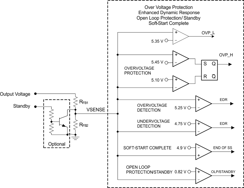 Figure 25. OVP_H, OVP_L, EDR, OLP, Soft Start Complete
8.3.10 Overcurrent Protection
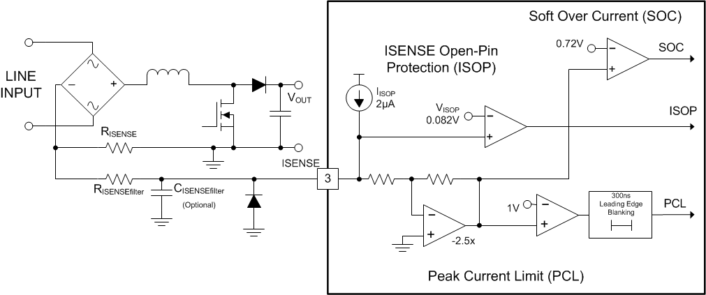
Inductor current is sensed by RISENSE, a low value resistor in the return path of input rectifier. The other side of the resistor is tied to the system ground. The voltage is sensed on the rectifier side of the sense resistor and is always negative. The voltage at ISENSE is buffered by a fixed gain of -2.5 to provide a positive internal signal to the current functions. There are two overcurrent protection features; Soft Overcurrent (SOC) protects against an overload on the output and Peak Current Limit (PCL) protects against inductor saturation.
8.3.11 Soft Overcurrent (SOC)
Soft Overcurrent (SOC) limits the input current. SOC is activated when the current sense voltage on ISENSE reaches –0.285 V. This is a soft control as it does not directly switch off the gate driver. Instead a 4-kΩ resistor connects VCOMP to ground to discharge VCOMP and the control loop is adjusted to reduce the PWM duty cycle. The under-voltage detection (UVD) is disabled during SOC.
8.3.12 Peak Current Limit (PCL)
Peak Current Limit (PCL) operates on a cycle-by-cycle basis. When the current sense voltage on ISENSE reaches –0.4 V, PCL is activated, immediately terminating the active switch cycle. PCL is leading-edge blanked to improve noise immunity against false triggering.
8.3.13 Current Sense Resistor, RISENSE
The current sense resistor, RISENSE, is sized using the minimum threshold value of Soft Over Current (SOC), VSOC(min) . To avoid triggering this threshold during normal operation, resulting in a decreased duty-cycle, the resistor is sized for an overload current of 10% more than the peak inductor current,

Since RISENSE “sees” the average input current, worst-case power dissipation occurs at input low-line when input current is at its maximum. Power dissipated by the sense resistor is given by:

Peak current limit (PCL) protection turns off the output driver when the voltage across the sense resistor reaches the PCL threshold, VPCL. The absolute maximum peak current, IPCL, is given by:

8.3.14 ISENSE Pin
The voltage at the ISENSE pin should be limited between 0 V and –1.1 V. Inrush currents at start-up have the potential to drive the ISENSE pin significantly more negative so a diode clamp should be used between ISENSE and GND to prevent the ISENSE pin going more negative than 1.1 V, (see Figure 26). The diode Vf should be greater than the maximum PCL threshold (–0.438 V) and less than –1.1 V across temperature and component variations.
8.3.15 Gate Driver
The GATE output is designed with a current-optimized structure to directly drive large values of total MOSFET/IGBT gate capacitance at high turn-on and turn-off speeds. An internal clamp limits voltage on the MOSFET gate to 15.2 V (typical). When VCC voltage is below the UVLO level, the GATE output is held in the off state. An external gate drive resistor, RGATE, can be used to limit the rise and fall times and dampen ringing caused by parasitic inductances and capacitances of the gate drive circuit and to reduce EMI. The final value of the resistor depends upon the parasitic elements associated with the layout and other considerations. A 10-kΩ resistor close to the gate of the MOSFET/IGBT, between the gate and ground, discharges stray gate capacitance and helps protect against inadvertent dv/dt-triggered turn-on.
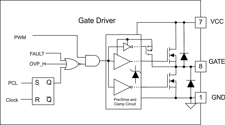 Figure 27. Gate Driver
8.3.16 Current Loop
The overall system current loop consists of the current averaging amplifier stage, the pulse width modulator (PWM) stage, the external boost inductor stage and the external current sensing resistor.
8.3.17 ISENSE and ICOMP Functions
The negative polarity signal from the current sense resistor is buffered and inverted at the ISENSE input. The internal positive signal is then averaged by the current amplifier (gmi), whose output is the ICOMP pin. The voltage on ICOMP is proportional to the average inductor current. An external capacitor to GND is applied to the ICOMP pin for current loop compensation and current ripple filtering. The gain of the averaging amplifier is determined by the internal VCOMP voltage. This gain is non-linear to accommodate the world-wide AC-line voltage range.
ICOMP is connected to 3-V internally whenever OVP_H, ISOP, or OLP is triggered.
8.3.18 Pulse Width Modulator
The PWM stage compares the ICOMP signal with a periodic ramp to generate a leading-edge-modulated output signal which is high whenever the ramp voltage exceeds the ICOMP voltage. The slope of the ramp is defined by a non-linear function of the internal VCOMP voltage.
The PWM output signal always starts low at the beginning of the cycle, triggered by the internal clock. The output stays low for a minimum off-time, tOFF_min, after which the ramp rises linearly to intersect the ICOMP voltage. The ramp-ICOMP intersection determines tOFF, and hence DOFF. Since DOFF = VIN/VOUT by the boost-topology equation, and since VIN is sinusoidal in wave-shape, and since ICOMP is proportional to the inductor current, it follows that the control loop forces the inductor current to follow the input voltage wave-shape to maintain boost regulation. Therefore, the average input current is also sinusoidal in wave-shape.
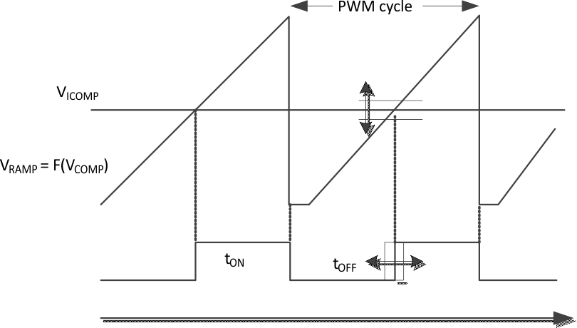 Figure 28. PWM Generation
8.3.19 Control Logic
The output of the PWM comparator stage is conveyed to the GATE drive stage, subject to control by various protection functions incorporated into the device. The GATE output duty-cycle may be as high as 98%, but always has a minimum off-time tOFF_min. Normal duty-cycle operation can be interrupted directly by OVP_H and PCL. UVLO, ISOP, ICOMMP and OLP/Standby also terminate the GATE output pulse, and further inhibit output until the SS operation can begin.
8.3.20 Voltage Loop
The outer control loop of the PFC controller is the voltage loop. This loop consists of the PFC output sensing stage, the voltage error amplifier stage, and the non-linear gain generation.
8.3.21 Output Sensing
A resistor-divider network from the PFC output voltage to GND forms the sensing block for the voltage control loop. The resistor ratio is determined by the desired output voltage and the internal 5-V regulation reference voltage.
The very low bias current at the VSENSE input allows the choice of the highest practicable resistor values for lowest power dissipation and standby current. A small capacitor from VSENSE to GND serves to filter the signal in a high-noise environment. This filter time constant should generally be less than 100 µs.
8.3.22 Voltage Error Amplifier
The transconductance error amplifier (gmv) generates an output current proportional to the difference between the voltage feedback signal at VSENSE and the internal 5-V reference. This output current charges or discharges the compensation network capacitors on the VCOMP pin to establish the proper VCOMP voltage for the system operating conditions. Proper selection of the compensation network components leads to a stable PFC pre-regulator over the entire AC-line range and 0% to 100% load range. The total capacitance also determines the rate-of-rise of the VCOMP voltage at Soft Start, as discussed earlier.
The amplifier output VCOMP is pulled to GND during any fault or standby condition to discharge the compensation capacitors to an initial zero state. Usually, the large capacitor has a series resistor which delays complete discharge for their respective time constant (which may be several hundred milliseconds). If VCC bias voltage is quickly removed after UVLO, the normal discharge transistor on VCOMP loses drive and the large capacitor could be left with substantial voltage on it, negating the benefit of a subsequent Soft Start. The UCC28180 incorporates a parallel discharge path which operates without VCC bias, to further discharge the compensation network after VCC is removed.
If the output voltage perturbations exceed ±5%, and output over-voltage (OVD) or under-voltage (UVD) is detected, the OVD or UVD function invokes EDR which immediately increases the voltage error amplifier transconductance to about 280 µS. This higher gain facilitates faster charging or discharging the compensation capacitors to the new operating level. When output voltage perturbations greater than 107%VREF appear at the VSENSE input, a 4-kΩ resistor connects VCOMP to ground to quickly reduce VCOMP voltage. When output voltage perturbations are greater than 109%VREF, the GATE output is shut off until VSENSE drops below 102% of regulation.
8.3.23 Non-Linear Gain Generation
The voltage at VCOMP is used to set the current amplifier gain and the PWM ramp slope. This voltage is subject to modification by the SOC function, as discussed earlier.
Together the current gain and the PWM slope adjust to the different system operating conditions (set by the AC-line voltage and output load level) as VCOMP changes, to provide a low-distortion, high-power-factor, input-current wave shape following that of the input voltage.
8.4 Device Functional Modes
This device has no functional modes.
