SLUSBQ5D November 2013 – July 2016 UCC28180
PRODUCTION DATA.
- 1 Features
- 2 Applications
- 3 Description
- 4 Revision History
- 5 Description (Continued)
- 6 Pin Configuration and Functions
- 7 Specifications
-
8 Detailed Description
- 8.1 Overview
- 8.2 Functional Block Diagram
- 8.3
Feature Description
- 8.3.1 Soft Start
- 8.3.2 System Protection
- 8.3.3 VCC Undervoltage LockOut (UVLO)
- 8.3.4 Output Overvoltage Protection (OVP)
- 8.3.5 Open Loop Protection/Standby (OLP/Standby)
- 8.3.6 ISENSE Open-Pin Protection (ISOP)
- 8.3.7 ICOMP Open-Pin Protection (ICOMPP)
- 8.3.8 FAULT Protection
- 8.3.9 Output Overvoltage Detection (OVD), Undervoltage Detection (UVD) and Enhanced Dynamic Response (EDR)
- 8.3.10 Overcurrent Protection
- 8.3.11 Soft Overcurrent (SOC)
- 8.3.12 Peak Current Limit (PCL)
- 8.3.13 Current Sense Resistor, RISENSE
- 8.3.14 ISENSE Pin
- 8.3.15 Gate Driver
- 8.3.16 Current Loop
- 8.3.17 ISENSE and ICOMP Functions
- 8.3.18 Pulse Width Modulator
- 8.3.19 Control Logic
- 8.3.20 Voltage Loop
- 8.3.21 Output Sensing
- 8.3.22 Voltage Error Amplifier
- 8.3.23 Non-Linear Gain Generation
- 8.4 Device Functional Modes
-
9 Application and Implementation
- 9.1 Application Information
- 9.2
Typical Application
- 9.2.1 Design Requirements
- 9.2.2
Detailed Design Procedure
- 9.2.2.1 Current Calculations
- 9.2.2.2 Switching Frequency
- 9.2.2.3 Bridge Rectifier
- 9.2.2.4 Inductor Ripple Current
- 9.2.2.5 Input Capacitor
- 9.2.2.6 Boost Inductor
- 9.2.2.7 Boost Diode
- 9.2.2.8 Switching Element
- 9.2.2.9 Sense Resistor
- 9.2.2.10 Output Capacitor
- 9.2.2.11 Output Voltage Set Point
- 9.2.2.12 Loop Compensation
- 9.2.3 Application Curve
- 10Power Supply Recommendations
- 11Layout
- 12Device and Documentation Support . .
- 13Mechanical, Packaging, and Orderable Information
Package Options
Mechanical Data (Package|Pins)
- D|8
Thermal pad, mechanical data (Package|Pins)
Orderable Information
11 Layout
11.1 Layout Guidelines
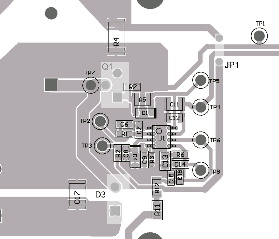
As with all PWM controllers, the effectiveness of the filter capacitors on the signal pins depends upon the integrity of the ground return. Separating the high di/dt induced noise on the power ground from the low current quiet signal ground is required for adequate noise immunity. Even with a signal layer PCB design, the pin out of the UCC28180 is ideally suited to minimize noise on the small signal traces. As shown in Figure 41, the capacitors on VSENSE, VCOMP, ISENSE, ICOMP, and FREQ (if used) must be all be returned directly to the portion of the ground plane that is the quiet signal GND and not in high-current return path of the converter, shown as power GND. The trace from the FREQ pin to the frequency programming resistor should be as short as possible. It is recommended that the compensation components on ICOMP and VCOMP are located as close as possible to the UCC28180. Placement of these components should take precedence, paying close attention to keeping their traces away from high noise areas. The bypass capacitors on VCC must be located physically close the VCC and GND pins of the UCC28180 but should not be in the immediate path of the signal return.
Other layout considerations should include keeping the switch node as short as possible, with a wide trace to reduce induced ringing caused by parasitic inductance. Every effort should be made to avoid noise from the switch node from corrupting the small signal traces with adequate clearance and ground shielding. As some compromises must be made due to limitation of PCB layers or space constraints, traces that must be made long, such as the signal from the current sense resistor shown in Figure 41, should be as wide as possible, avoid long narrow traces.
