SLUSA12G December 2009 – November 2022 UCC28C40-Q1 , UCC28C41-Q1 , UCC28C42-Q1 , UCC28C43-Q1 , UCC28C44-Q1 , UCC28C45-Q1
PRODUCTION DATA
- 1 Features
- 2 Applications
- 3 Description
- 4 Revision History
- 5 Device Comparison Table
- 6 Pin Configuration and Functions
- 7 Specifications
-
8 Detailed Description
- 8.1 Overview
- 8.2 Functional Block Diagram
- 8.3 Feature Description
- 8.4 Device Functional Modes
-
9 Application and Implementation
- 9.1 Application Information
- 9.2
Typical Application
- 9.2.1 Design Requirements
- 9.2.2
Detailed Design Procedure
- 9.2.2.1 Custom Design With WEBENCH® Tools
- 9.2.2.2 Input Bulk Capacitor and Minimum Bulk Voltage
- 9.2.2.3 Transformer Turns Ratio and Maximum Duty CycleG
- 9.2.2.4 Transformer Inductance and Peak Currents
- 9.2.2.5 Output Capacitor
- 9.2.2.6 Current Sensing Network
- 9.2.2.7 Gate Drive Resistor
- 9.2.2.8 VREF Capacitor
- 9.2.2.9 RT/CT
- 9.2.2.10 Start-Up Circuit
- 9.2.2.11 Voltage Feedback Compensation
- 9.2.3 Application Curves
- 9.2.4 Power Supply Recommendations
- 9.2.5 Layout
- 10Device and Documentation Support
- 11Mechanical, Packaging, and Orderable Information
Package Options
Mechanical Data (Package|Pins)
- D|8
Thermal pad, mechanical data (Package|Pins)
Orderable Information
8.3.4 Current Sense and Overcurrent Limit
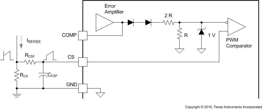
An external series resistor (RCS) senses the current and converts this current into a voltage that becomes the input to the CS pin. The CS pin is the noninverting input to the PWM comparator. The CS input is compared to a signal proportional to the error amplifier output voltage; the gain of the current sense amplifier is typically 3 V/V. The peak ISENSE current is determined using Equation 2

The typical value for VCS is 1 V. A small RC filter (RCSF and CCSF) may be required to suppress switch transients caused by the reverse recovery of a secondary side diode or equivalent capacitive loading in addition to parasitic circuit impedances. The time constant of this filter should be considerably less than the switching period of the converter.
 Figure 8-3 Current-Sense Circuit Schematic
Cycle-by-cycle pulse width modulation performed at the PWM comparator essentially compares the error amplifier output to the current sense input. This is not a direct volt-to-volt comparison, as the error amplifier output network incorporates two diodes in series with a resistive divider network before connecting to the PWM comparator. The two-diode drop adds an offset voltage that enables zero duty cycle to be achieved with a low amplifier output. The 2R/R resistive divider facilitates the use of a wider error amplifier output swing that can be more symmetrically centered on the 2.5-V noninverting input voltage.
The 1-V zener diode associated with the PWM comparator’s input from the error amplifier is not an actual diode in the device’s design, but an indication that the maximum current sense input amplitude is 1 V (typical). When this threshold is reached, regardless of the error amplifier output voltage, cycle-by-cycle current limiting occurs, and the output pulse width is terminated within 35 ns (typical). The minimum value for this current limit threshold is 0.9 V with a 1.1-V maximum. In addition to the tolerance of this parameter, the accuracy of the current sense resistor, or current sense circuitry, must be taken into account. It is advised to factor in the worst case of primary and secondary currents when sizing the ratings and worst-case conditions in all power semiconductors and magnetic components.