SLUSC18A September 2014 – March 2015 UCC29950
PRODUCTION DATA.
- 1 Features
- 2 Applications
- 3 Description
- 4 Revision History
- 5 Pin Configuration and Functions
- 6 Specifications
-
7 Detailed Description
- 7.1 Overview
- 7.2 Functional Block Diagram
- 7.3
Feature Description
- 7.3.1 Sense Networks
- 7.3.2 Sense Network Fault Detection
- 7.3.3 PFC Stage Soft-Start
- 7.3.4 AC Line Voltage Sensing
- 7.3.5 VBLK Sensing
- 7.3.6 AC Input UVLO and Brownout Protection
- 7.3.7 Dither
- 7.3.8 Active X-Cap Discharge
- 7.3.9 LLC Stage Soft Start
- 7.3.10 PFC Stage Current Sensing
- 7.3.11 Input Power Limit
- 7.3.12 PFC Stage Soft Start
- 7.3.13 Hybrid PFC Control Loop
- 7.3.14 PFC Stage Second Current Limit
- 7.3.15 PFC Inductor and Bulk Capacitor Recommendations
- 7.3.16 PFC Stage Over Voltage Protection
- 7.3.17 LLC Stage Control
- 7.3.18 Driver Output Stages and Characteristic
- 7.3.19 LLC Stage Dead Time Profile
- 7.3.20 LLC Stage Current Sensing
- 7.3.21 LLC Three Level Over-Current Protection
- 7.3.22 Over-Temperature Protection
- 7.3.23 Fault Timer and Control
- 7.4 Device Functional Modes
-
8 Application and Implementation
- 8.1 Application Information
- 8.2
Typical Application
- 8.2.1 Design Requirements
- 8.2.2
Detailed Design Procedure
- 8.2.2.1 LLC Stage
- 8.2.2.2 LLC Switching Frequency
- 8.2.2.3 LLC Transformer Turns Ratio
- 8.2.2.4 LLC Stage Equivalent Load Resistance
- 8.2.2.5 LLC Gain Range
- 8.2.2.6 Select LN and QE
- 8.2.2.7 LLC No-Load Gain
- 8.2.2.8 Parameters of the LLC Resonant Circuit
- 8.2.2.9 Verify the LLC Resonant Circuit Design
- 8.2.2.10 LLC Primary-Side Currents
- 8.2.2.11 LLC Secondary-Side Currents
- 8.2.2.12 LLC Transformer
- 8.2.2.13 LLC Resonant Inductor
- 8.2.2.14 Combining the LLC Resonant Inductor and Transformer
- 8.2.2.15 LLC Resonant Capacitor
- 8.2.2.16 LLC Stage with Split Resonant Capacitor
- 8.2.2.17 LLC Primary-Side MOSFETs
- 8.2.2.18 LLC Output Rectifier Diodes
- 8.2.2.19 LLC Stage Output Capacitors
- 8.2.2.20 LLC Stage Over-Current Protection, Current Sense Resistor
- 8.2.2.21 Detailed Design Procedure for the PFC stage
- 8.2.2.22 PFC Stage Output Current Calculation
- 8.2.2.23 Line Current Calculation
- 8.2.2.24 Bridge Rectifier
- 8.2.2.25 PFC Boost Inductor
- 8.2.2.26 PFC Input Capacitor
- 8.2.2.27 PFC Stage MOSFET
- 8.2.2.28 PFC Boost Diode
- 8.2.2.29 Bulk Capacitor
- 8.2.2.30 PFC Stage Current Sense Resistor
- 8.2.3 Application Curves
- 8.3 Do's and Don'ts
- 9 Power Supply Recommendations
- 10Layout
- 11Device and Documentation Support
- 12Mechanical, Packaging, and Orderable Information
Package Options
Mechanical Data (Package|Pins)
- D|16
Thermal pad, mechanical data (Package|Pins)
Orderable Information
1 Features
- High Efficiency PFC and Half-Bridge Resonant LLC Combo Controller
- Continuous Conduction Mode (CCM) Boost Power Factor Correction
- Supports Self-Bias or Auxiliary (external) Bias Mode of Operation
- PFC Loops Fully Internally Compensated
- PFC Stage Design in 3 Easy Steps
(design voltage feedback, current feedback and power stage) - Fixed 100-kHz PFC Frequency with Dithering for Ease of EMI Compliance
- True Input Power Limit, Independent of Line Voltage
- Fixed LLC Frequency Operating Range of 70 kHz to 350 kHz
- Dead-Time Varied Across Load Range for LLC Half-Bridge Power Stage to Extend ZVS Range
- Three-Level LLC Over-Current Protection
- Hiccup Mode Operation for Continuous Overload and Short-Circuit Power Protection
- Low Standby Power Consumption Enabled by Active Control of High-Voltage Start-Up MOSFET and X-Cap Discharge Function
- Built In Soft-Start and Converter Sequencing to Simplify Design
- AC Line Brownout Protection, with Fail Indicator
- PFC Bus Over-Voltage and Under-Voltage Protection
- Over-Temperature Protection
- External Gate Drivers for Scalability with Power Level
- SOIC-16 Package
2 Applications
- Offline AC-to-DC Server Power Supplies (80 PLUS® Bronze/Silver/Gold)
- Industrial DIN Rail and Open Frame Power Supplies
- Gaming and Printer Power
- High-Density Adapters
- Lighting Drivers
3 Description
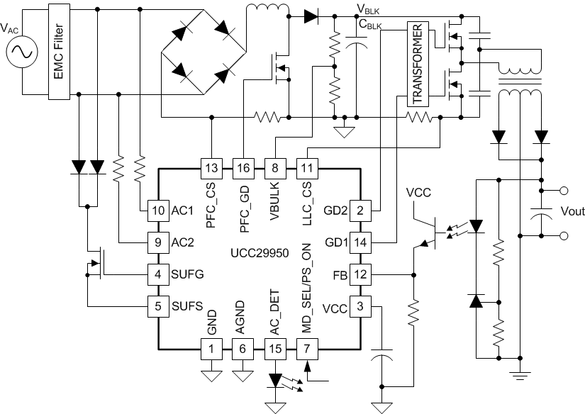
The UCC29950 provides all the control functionality for an AC-to-DC converter with a CCM boost Power Factor Correction (PFC) stage followed by an LLC converter stage. The controller is optimized to allow ease of use.
Proprietary CCM PFC algorithms enable the system to achieve high efficiency, smaller converter size with high power factor. The integrated LLC controller enables a high-efficiency DC-to-DC conversion stage utilizing soft switching for low EMI noise. Integration of PFC control and LLC control in a combo controller allows the control algorithms to take advantage of information from both stages.
The controller includes a control circuit for start-up using a Depletion Mode MOSFET with internal device power management that minimizes external component requirements and helps lower system implementation costs.
To further reduce the standby power an X-Cap discharge circuit is integrated. The UCC29950 implements a complete suite of system protection functions, including AC line brownout, PFC bus under voltage PFC and LLC, over current and thermal shutdown.
Device Information(1)
| PART NUMBER | PACKAGE | BODY SIZE (NOM) |
|---|---|---|
| UCC29950 | SOIC 16 Pin (D) | 9.90 mm x 6.00 mm |
- For all available packages, see the orderable addendum at the end of the datasheet.
Simplified Schematic

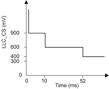
LLC stage Over-Current Protection Profile
