SLVSC86A January 2014 – March 2014 UCD9244-EP
PRODUCTION DATA.
- 1 Features
- 2 Applications
- 3 Description
- 4 Revision History
- 5 Description (Continued)
- 6 Terminal Configuration and Functions
-
7 Specifications
- 7.1 Absolute Maximum Ratings
- 7.2 Handling Ratings
- 7.3 Recommended Operating Conditions
- 7.4 Thermal Information
- 7.5 Electrical Characteristics
- 7.6 Electrical Characteristics (Continued)
- 7.7 ADC Monitoring Intervals And Response Times
- 7.8 Hardware Fault Detection Latency
- 7.9 PMBus/SMBus/I2C
- 7.10 I2C/SMBus/PMBus Timing Requirements
- 7.11 Typical Characteristics
-
8 Detailed Description
- 8.1 Overview
- 8.2 Functional Block Diagram
- 8.3
Feature Description
- 8.3.1 PMBus Interface
- 8.3.2 Resistor Programmed PMBus Address Decode
- 8.3.3 VID Interface
- 8.3.4 Jtag Interface
- 8.3.5 Bias Supply Generator (Shunt Regulator Controller)
- 8.3.6 Power-On Reset
- 8.3.7 External Reset
- 8.3.8 ON_OFF_CONFIG
- 8.3.9 Output Voltage Adjustment
- 8.3.10 Calibration
- 8.3.11 Analog Front End (AFE)
- 8.3.12 Voltage Sense Filtering
- 8.3.13 DPWM Engine
- 8.3.14 Rail/Power Stage Configuration
- 8.3.15 DPWM Phase Synchronization
- 8.3.16 Output Current Measurement
- 8.3.17 Current Sense Input Filtering
- 8.3.18 Over-Current Detection
- 8.3.19 Input Voltage Monitoring
- 8.3.20 Input UV Lockout
- 8.3.21 Temperature Monitoring
- 8.3.22 Auxiliary ADC Input Monitoring
- 8.3.23 Soft Start, Soft Stop Ramp Sequence
- 8.3.24 Non-Volatile Memory Error Correction Coding
- 8.3.25 Data Logging
- 8.4 Device Functional Modes
- 9 Applications and Implementation
- 10Power Supply Recommendations
- 11Layout
- 12Device and Documentation Support
- 13Mechanical, Packaging, and Orderable Information
Package Options
Mechanical Data (Package|Pins)
- RGC|64
Thermal pad, mechanical data (Package|Pins)
- RGC|64
Orderable Information
8.4.2 6-Bit VID Mode
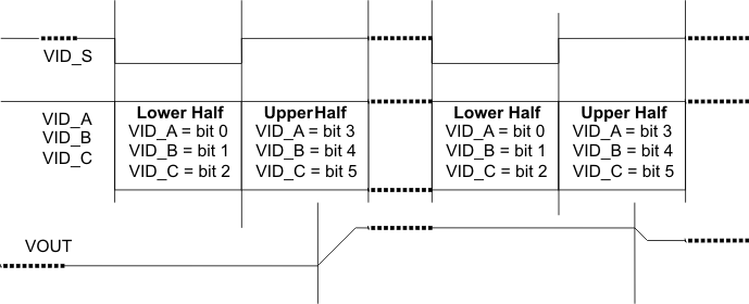
In 6-bit VID mode, the four VID input signals are used to provide the six bits of VID data, as shown in the table below. Each of the three data lines (VID_A, VID_B, and VID_C) carries two bits of data per VID code. The bits are clocked and selected by the VID_S select line.
| TERMINAL | PURPOSE | RAIL 1 | RAIL 2 | RAIL 3 | RAIL 4 |
|---|---|---|---|---|---|
| VID_A | Data bit 0 when VID_S is low, Data bit 3 when VID_S is high |
VID1A | VID2A | VID3A | VID4A |
| VID_B | Data bit 1 when VID_S is low, Data bit 4 when VID_S is high |
VID1B | VID2B | VID3B | VID4B |
| VID_C | Data bit 2 when VID_S is low, Data bit 5 when VID_S is high |
VID1C | VID2C | VID3C | VID4C |
| VID_S | Select Line: Low= LSB, High = MSB |
VID1S | VID2S | VID3S | VID4S |
The falling edge of the VID_S line triggers the UCD9244 to read bits 2:0 on the three VID data lines. The rising edge of VID_S triggers the UCD9244 to read bits 5:3 on the three VID data lines and calculate a new VOUT setpoint. This calculation takes from 35 to 135µs. The output voltage will then slew to the new setpoint voltage at the rate specified by the VOUT_TRANSITION_RATE PMBus command.
 Figure 14. 6-Bit VID Data Transfer
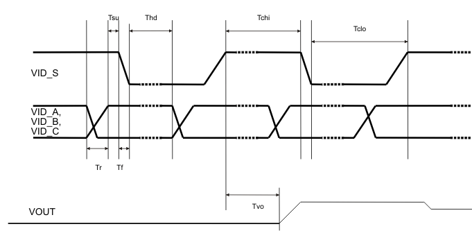
The set-up time on the data lines is 0 µs. All four VID lines must hold at the same level for some time after a change in the VID_S line to allow the UCD9244 to read and validate the data signals and perform necessary voltage calculations. The UCD9244 can tolerate single hold times as short as 70µs, but does not have sufficient computation power to sustain continuous VID messaging that quickly. It is expected that the hold time will be at least 125µs for sustained operations. It is recommended that the DSP only send VID messages when the regulated voltage needs to change; sending the same VID code repeatedly and continuously provides no benefit.
Figure 15 and Table 6 illustrate the critical timing measurements as they apply to the 6-bit VID interface.
 Figure 15. 6-Bit VID Timing
Table 6. 6-Bit VID Timing
| SYMBOL | PARAMETER | MIN | TYP | MAX | UNITS |
|---|---|---|---|---|---|
| Tr | Data and clock rise time | – | 2.5 | µs | |
| Tf | Data and clock fall time | – | 0.3 | µs | |
| Tsu | Data setup before changing clock | 0 | µs | ||
| Thd | Data hold until next clock change | 70 | µs | ||
| Tchi | Clock high time | 70 | 125 | µs | |
| Tclo | Clock low time | 70 | 125 | µs | |
| Tvo | Response time from rising edge of VID_S to start of Vout slewing to new setpoint | 35 | 135 | µs |