SLRS027T December 1976 – March 2025 ULN2002A , ULN2003A , ULN2003AI , ULN2004A , ULQ2003A , ULQ2004A
PRODUCTION DATA
- 1
- 1 Features
- 2 Applications
- 3 Description
- 4 Pin Configuration and Functions
-
5 Specifications
- 5.1 Absolute Maximum Ratings
- 5.2 ESD Ratings
- 5.3 Recommended Operating Conditions
- 5.4 Thermal Information
- 5.5 Electrical Characteristics: ULN2002A
- 5.6 Electrical Characteristics: ULN2003A and ULN2004A
- 5.7 Electrical Characteristics: ULN2003AI
- 5.8 Electrical Characteristics: ULN2003AI
- 5.9 Electrical Characteristics: ULQ2003A and ULQ2004A
- 5.10 Switching Characteristics: ULN2002A, ULN2003A, ULN2004A
- 5.11 Switching Characteristics: ULN2003AI
- 5.12 Switching Characteristics: ULN2003AI
- 5.13 Switching Characteristics: ULQ2003A, ULQ2004A
- 5.14 Typical Characteristics
- 6 Parameter Measurement Information
- 7 Detailed Description
- 8 Application and Implementation
- 9 Device and Documentation Support
- 10Revision History
- 11Mechanical, Packaging, and Orderable Information
Package Options
Refer to the PDF data sheet for device specific package drawings
Mechanical Data (Package|Pins)
- PW|16
- DYY|16
- NS|16
- N|16
- D|16
Thermal pad, mechanical data (Package|Pins)
Orderable Information
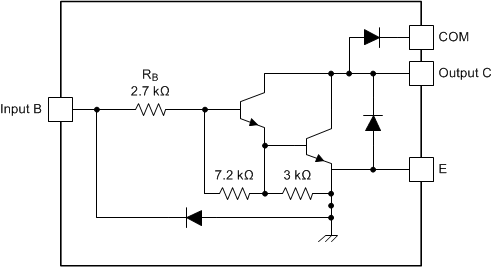
7.2 Functional Block Diagrams
All resistor values shown are nominal. The collector-emitter diode is a parasitic structure and should not be used to conduct current. If the collectors go below GND, an external Schottky diode should be added to clamp negative undershoots.
 Figure 7-1 ULN2002A Block
Diagram
 Figure 7-2 ULN2003A, ULQ2003A and ULN2003AI Block Diagram
 Figure 7-3 ULN2004A and LQ2004A Block Diagram