SWRS286 May 2021 WL1801 , WL1831
PRODUCTION DATA
- 1Features
- 2Applications
- 3Description
- 4System Block Diagram
- 5Chip Packaging and Ordering
- 6Mechanical Drawing
Package Options
Mechanical Data (Package|Pins)
- YFV|130
Thermal pad, mechanical data (Package|Pins)
Orderable Information
6 Mechanical Drawing
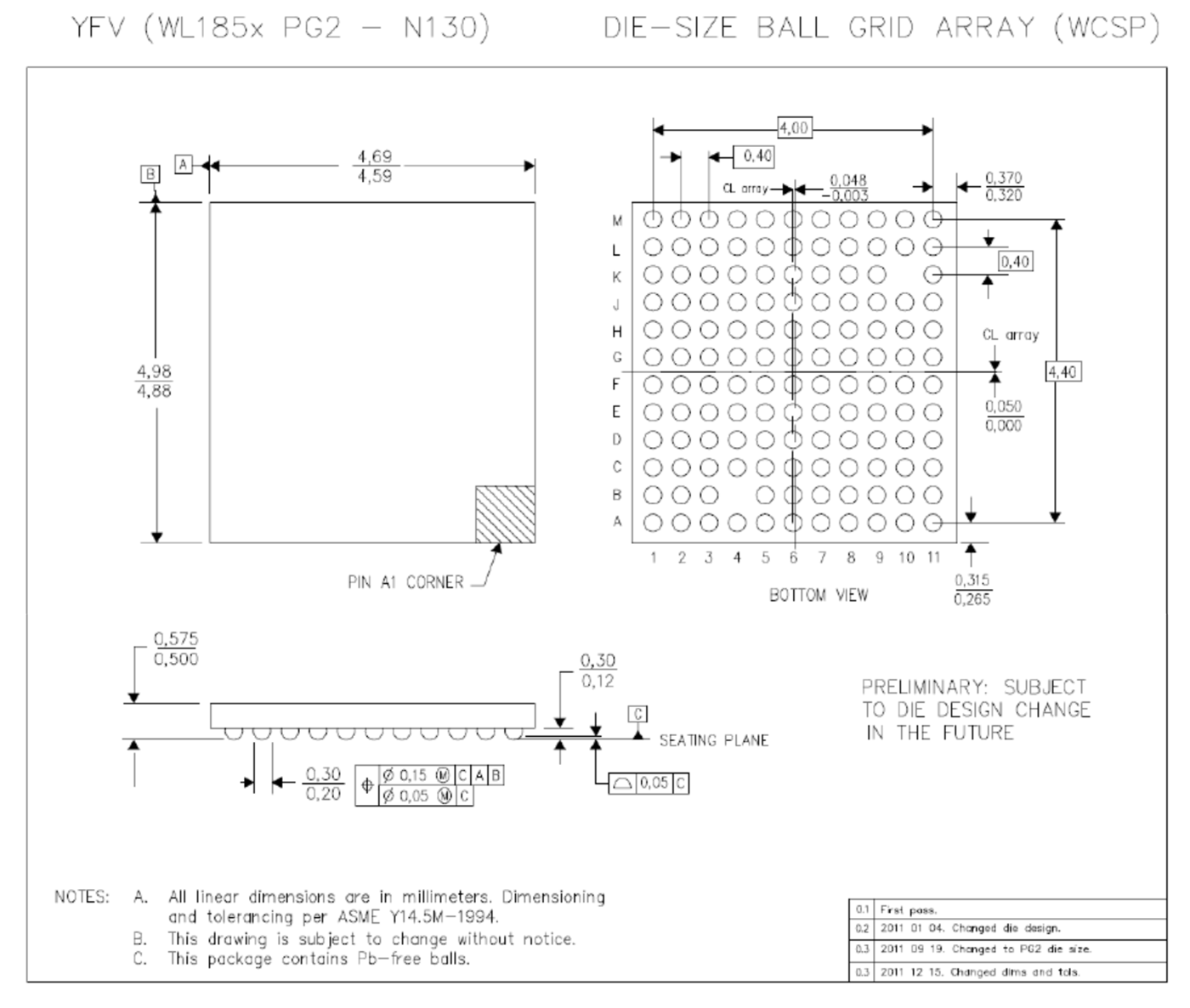
| DESCRIPTION | MIN | NOM | MAX |
|---|---|---|---|
| Body size (W, mm) * | 4.59 | 4.64 | 4.69 |
| Body size (L, mm) * | 4.88 | 4.93 | 4.98 |
| Overall thickness (t, mm) | 0.500 | 0.538 | 0.575 |
| Terminal pitch (mm) | ----- | 0.40 | ----- |
| Ball / terminal diameter (mm) | 0.20 | 0.25 | 0.30 |
| Ball height (mm) | 0.12 | 0.21 | 0.30 |
| Ball matrix footprint (W x L) | ----- | 11x12 | ----- |
| Coplanarity at terminal / ball side (mm) | ----- | ----- | 0.05 |