SNLS407D April 2012 – October 2014 DS90UB925Q-Q1
PRODUCTION DATA.
- 1 Features
- 2 Applications
- 3 Description
- 4 Revision History
- 5 Pin Configuration and Functions
- 6 Specifications
-
7 Detailed Description
- 7.1 Overview
- 7.2 Functional Block Diagram
- 7.3
Feature Description
- 7.3.1 High Speed Forward Channel Data Transfer
- 7.3.2 Low Speed Back Channel Data Transfer
- 7.3.3 Backward Compatible Mode
- 7.3.4 Common Mode Filter Pin (CMF)
- 7.3.5 Video Control Signal Filter
- 7.3.6 EMI Reduction Features
- 7.3.7 LVCMOS VDDIO Option
- 7.3.8 Power Down (PDB)
- 7.3.9 Remote Auto Power Down Mode
- 7.3.10 Input PCLK Loss Detect
- 7.3.11 Serial Link Fault Detect
- 7.3.12 Pixel Clock Edge Select (RFB)
- 7.3.13 Low Frequency Optimization (LFMODE)
- 7.3.14 Interrupt Pin — Functional Description And Usage (INTB)
- 7.3.15 Internal Pattern Generation
- 7.3.16 GPIO[3:0] and GPO_REG[8:4]
- 7.3.17 I2S Transmitting
- 7.3.18 Built In Self Test (BIST)
- 7.4 Device Functional Modes
- 7.5 Programming
- 7.6 Register Maps
- 8 Application and Implementation
- 9 Power Supply Recommendations
- 10Layout
- 11Device and Documentation Support
- 12Mechanical, Packaging, and Orderable Information
Package Options
Mechanical Data (Package|Pins)
- RHS|48
Thermal pad, mechanical data (Package|Pins)
- RHS|48
Orderable Information
1 Features
- Bidirectional Control Interface Channel Interface with I2C Compatible Serial Control Bus
- Supports High Definition (720 p) Digital Video Format
- RGB888 + VS, HS, DE and I2S Audio Supported
- Supports Two 10–bit Camera Video Streams
- 5 – 85MHz PCLK Supported
- Single 3.3 V Operation with 1.8 V or 3.3 V Compatible LVCMOS I/O Interface
- AC-Coupled STP Interconnect Up to 10 Meters
- Parallel LVCMOS Video Inputs
- DC-Balanced and Scrambled Data with Embedded Clock
- Supports Repeater Application
- Internal Pattern Generation
- Low Power Modes Minimize Power Dissipation
- Automotive Grade Product: AEC-Q100 Grade 2 Qualified
- >8kV HBM and ISO 10605 ESD Rating
- Backward Compatible to FPD-Link II
2 Applications
- Automotive Display for Navigation
- Rear Seat Entertainment Systems
- Automotive Driver Assistance
- Automotive Megapixel Camera Systems
3 Description
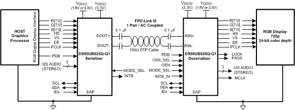
The DS90UB925Q-Q1 serializer, in conjunction with the DS90UB926Q-Q1 deserializer, provides a complete digital interface for concurrent transmission of high-speed video, audio, and control data for automotive display and image sensing applications.
The chipset is ideally suited for automotive video-display systems with HD formats and automotive vision systems with megapixel resolutions. The DS90UB925Q-Q1 incorporates an embedded bidirectional control channel and low latency GPIO controls. This chipset translates a parallel interface into a single pair high-speed serialized interface. The serial bus scheme, FPD-Link III, supports full duplex of high-speed video data transmission and bidirectional control communication over a single differential link. Consolidation of video data and control over a single differential pair reduces the interconnect size and weight, while also eliminating skew issues and simplifying system design.
The DS90UB925Q-Q1 serializer embeds the clock, DC scrambles & balances the data payload, and level shifts the signals to high-speed low voltage differential signaling. Up to 24 data bits are serialized along the video control signals.
Serial transmission is optimized by a user selectable de-emphasis. EMI is minimized by the use of low voltage differential signaling, data scrambling and randomization and spread spectrum clocking compatibility.
- For all available packages, see the orderable addendum at the end of the data sheet.