JAJSM24A December 2023 – May 2024 ADC3910D125
PRODUCTION DATA
- 1
- 1 特長
- 2 アプリケーション
- 3 概要
- 4 Pin Configuration and Functions
-
5 Specifications
- 5.1 Absolute Maximum Ratings
- 5.2 ESD Ratings
- 5.3 Recommended Operating Conditions
- 5.4 Thermal Information
- 5.5 Electrical Characteristics - Power Consumption
- 5.6 Electrical Characteristics - DC Specifications
- 5.7 Electrical Characteristics - AC Specifications (25 MSPS)
- 5.8 Electrical Characteristics - AC Specifications (65 MSPS)
- 5.9 Electrical Characteristics - AC Specifications (125 MSPS)
- 5.10 Timing Requirements
- 5.11 Output Interface Timing Diagram
- 5.12 Typical Characteristics - 25MSPS
- 5.13 Typical Characteristics - 65MSPS
- 5.14 Typical Characteristics - 125MSPS
-
6 Detailed Description
- 6.1 Overview
- 6.2 Functional Block Diagram
- 6.3 Feature Description
- 6.4 Device Functional Modes
- 6.5 Programming
- 6.6 Register Maps
- 7 Application Information Disclaimer
- 8 Device and Documentation Support
- 9 Revision History
- 10Mechanical, Packaging, and Orderable Information
6.3.6.1.2 Decimation Filter
The ADC3910Dx および ADC3910Sx has a stop band rejection of at least 70dB, and a pass-band bandwidth of approximately 80%. Table 6-2 gives an overview of the pass-band bandwidth of the different decimation settings with respect to ADC sampling rate FS.
| REAL DECIMATION | DECIMATION SETTING (N) | OUTPUT RATE | OUTPUT BANDWIDTH | OUTPUT RATE (FS = 125MSPS) |
OUTPUT BANDWIDTH (FS = 125MSPS) |
|---|---|---|---|---|---|
| Real | 2 | FS / 2 | 0.8 × FS / (2 × 2) | 62.5MSPS | 25MHz |
| 4 | FS / 4 | 0.8 × FS / (4 × 2) | 31.25MSPS | 12.5MHz | |
| 8 | FS / 8 | 0.8 × FS / (8 × 2) | 15.625MSPS | 6.25MHz | |
| 16 | FS / 16 | 0.8 × FS / (16 × 2) | 7.8125MSPS | 3.125MHz |
The decimation filter responses are normalized to the ADC sampling clock frequency FS and illustrated in Figure 6-12 to Figure 6-19. They are interpreted as follows:
Each figure contains the filter pass-band, transition band(s) and alias or stop-band(s) as shown in Figure 6-11. The x-axis shows the offset frequency normalized to the ADC sampling rate FS.
For example, in the divide-by-4 setup, the output data rate is FS / 4 with a Nyquist zone of FS / 8 or 0.125 × FS. The transition band (colored in blue) is centered around 0.125 × FS and the alias transition band is centered at 0.375 × FS. The stop-bands (colored in red), which alias on top of the pass-band, are centered at 0.25 × FS and 0.5 × FS.
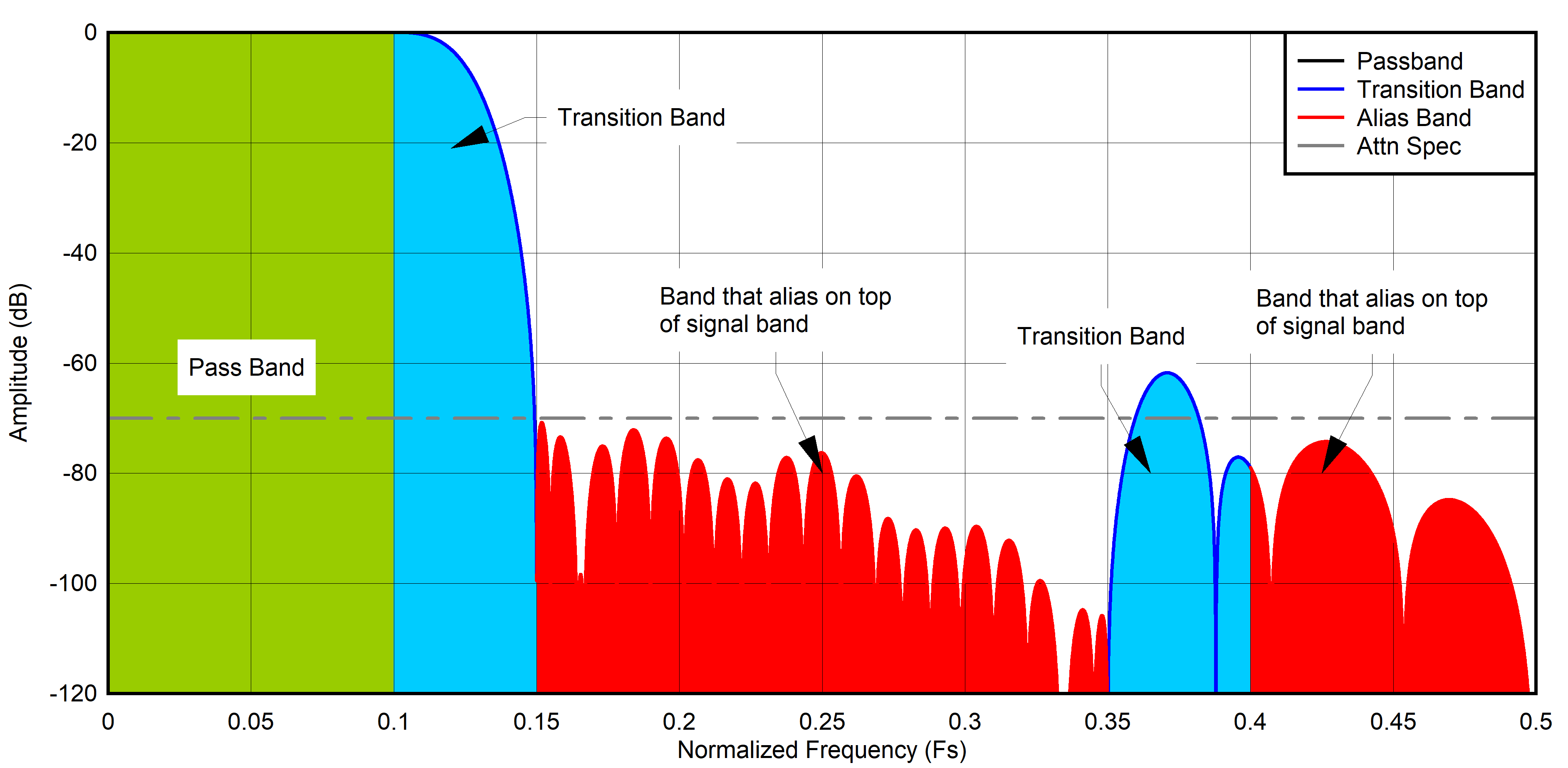 Figure 6-11 Interpretation of the
Decimation Filter Plots
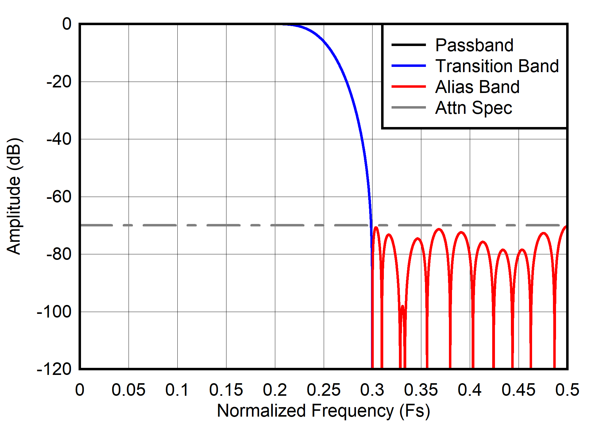 Figure 6-12 Decimation by 2 frequency
response
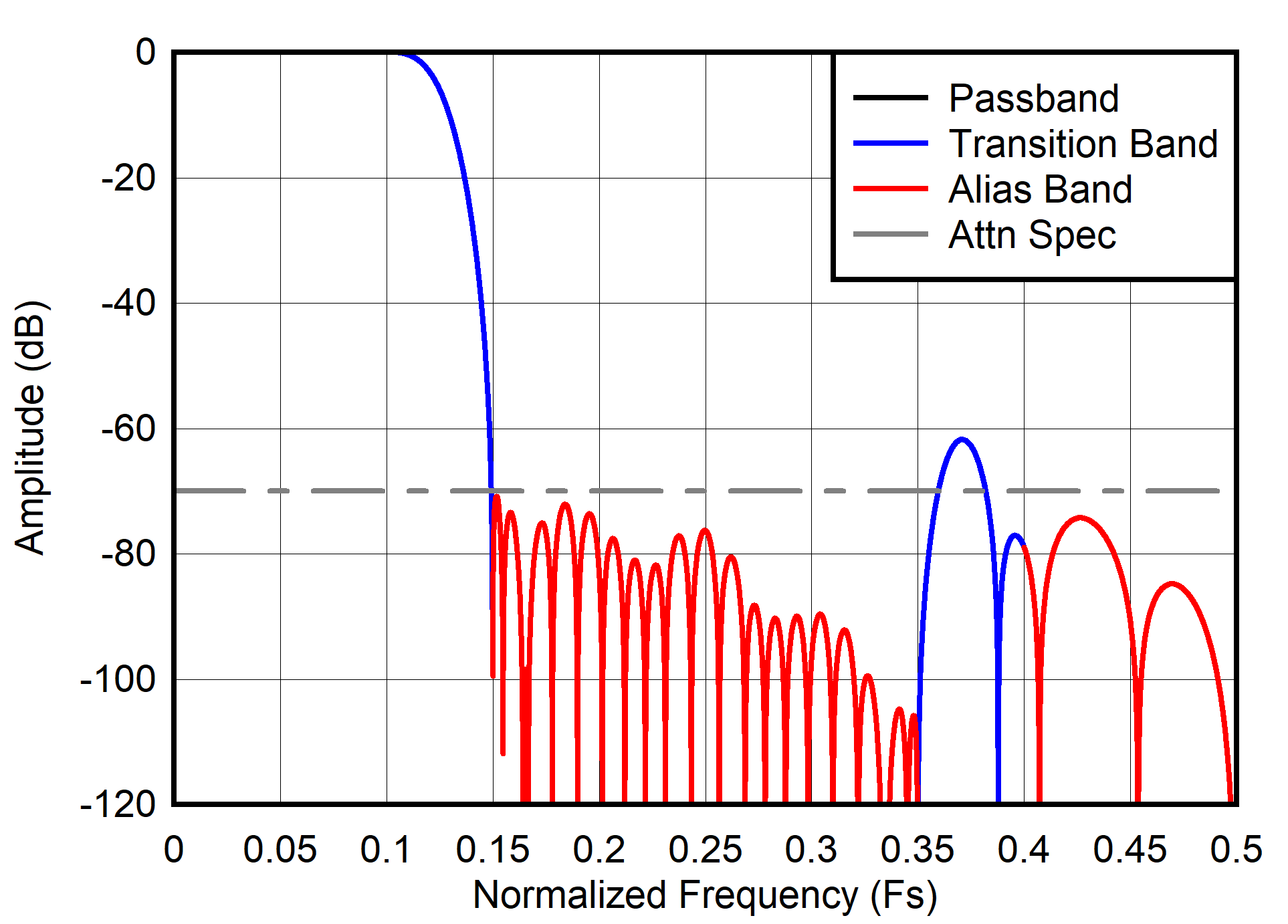 Figure 6-14 Decimation by 4 frequency
response
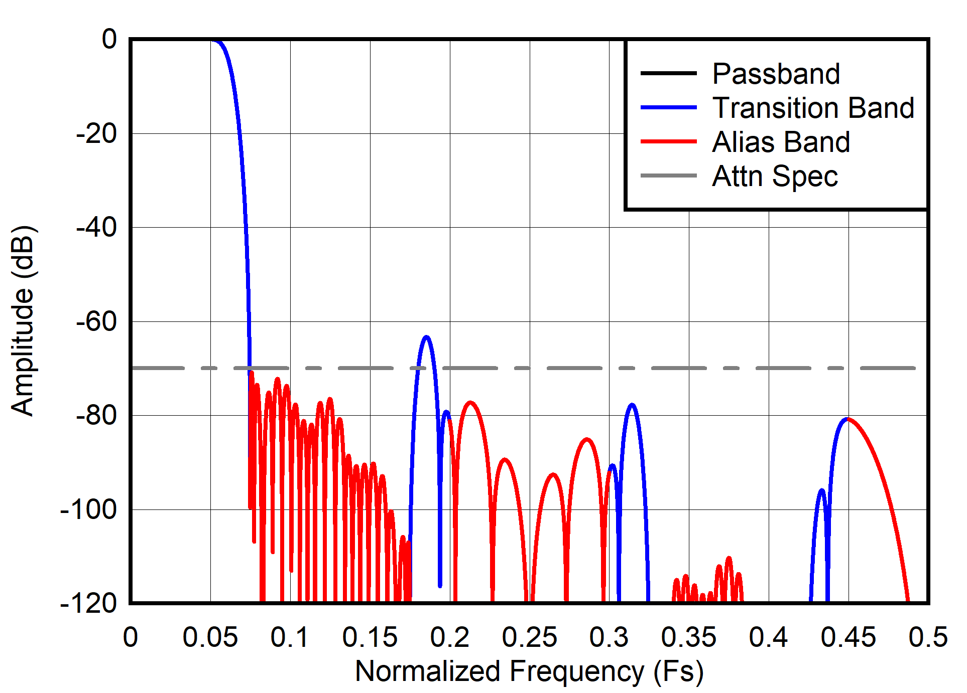 Figure 6-16 Decimation by 8 frequency
response
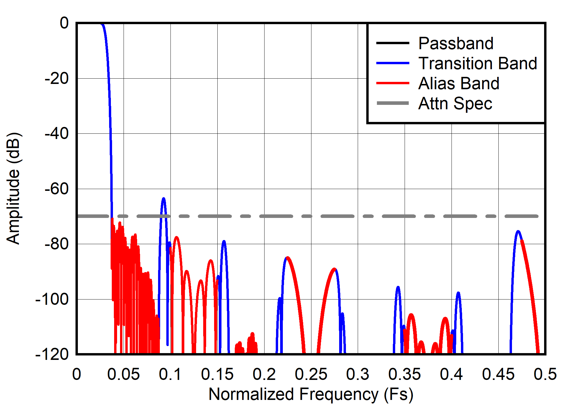 Figure 6-18 Decimation by 16 frequency
response
| FIN = 1 MHz, AIN = -1dBFS, 16-bit resolution mode |
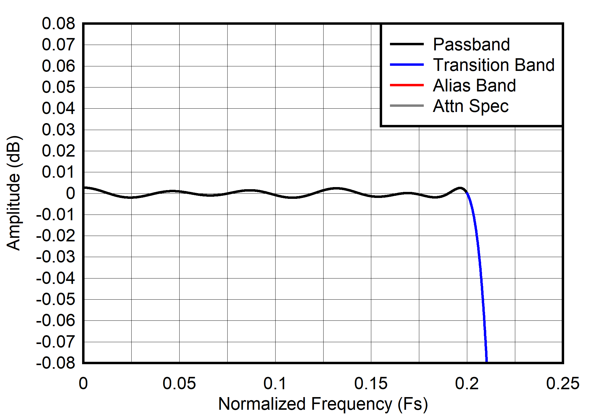 Figure 6-13 Decimation by 2 passband
ripple response
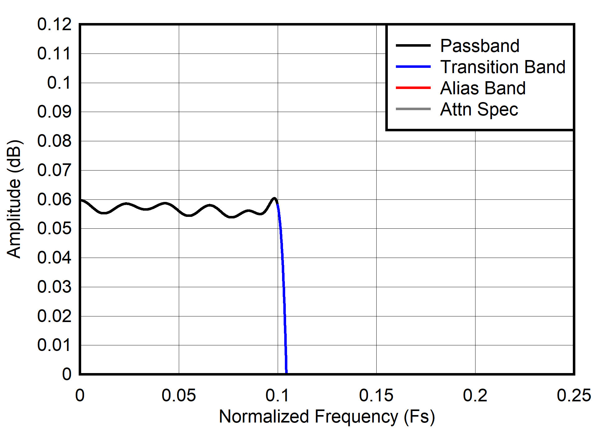 Figure 6-15 Decimation by 4 passband
ripple response
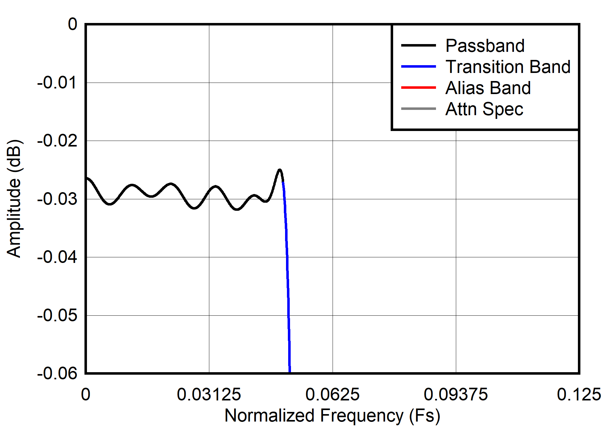 Figure 6-17 Decimation by 8 passband
ripple response
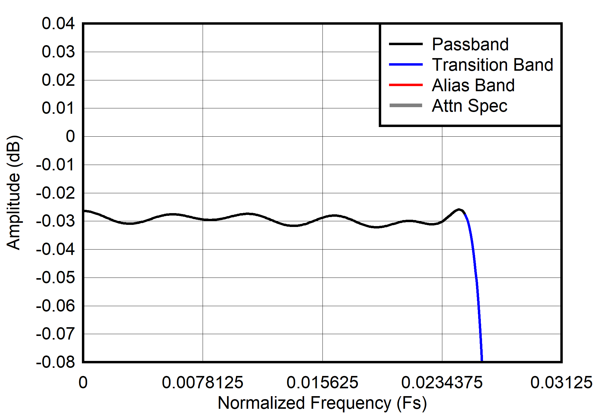 Figure 6-19 Decimation by 16 passband
ripple response