JAJSP39A May 2022 – December 2022 ADS1285
PRODUCTION DATA
- 1 特長
- 2 アプリケーション
- 3 概要
- 4 Revision History
- 5 Pin Configuration and Functions
-
6 Specifications
- 6.1 Absolute Maximum Ratings
- 6.2 ESD Ratings
- 6.3 Recommended Operating Conditions
- 6.4 Thermal Information
- 6.5 Electrical Characteristics
- 6.6 Timing Requirements: 1.65 V ≤ IOVDD ≤ 1.95 V and 2.7 V ≤ IOVDD ≤ 3.6 V
- 6.7 Switching Characteristics: 1.65V ≤ IOVDD ≤ 1.95V and 2.7 V ≤ IOVDD ≤ 3.6 V
- 6.8 Timing Diagrams
- 6.9 Typical Characteristics
- 7 Parameter Measurement Information
-
8 Detailed Description
- 8.1 Overview
- 8.2 Functional Block Diagram
- 8.3 Feature Description
- 8.4 Device Functional Modes
- 8.5
Programming
- 8.5.1 Serial Interface
- 8.5.2 Conversion Data Format
- 8.5.3
Commands
- 8.5.3.1 Single Byte Command
- 8.5.3.2 WAKEUP: Wake Command
- 8.5.3.3 STANDBY: Software Power-Down Command
- 8.5.3.4 SYNC: Synchronize Command
- 8.5.3.5 RESET: Reset Command
- 8.5.3.6 Read Data Direct
- 8.5.3.7 RDATA: Read Conversion Data Command
- 8.5.3.8 RREG: Read Register Command
- 8.5.3.9 WREG: Write Register Command
- 8.5.3.10 OFSCAL: Offset Calibration Command
- 8.5.3.11 GANCAL: Gain Calibration Command
- 8.6
Register Map
- 8.6.1
Register Descriptions
- 8.6.1.1 ID/SYNC: Device ID, SYNC Register (Address = 00h) [Reset = xxxx0000b]
- 8.6.1.2 CONFIG0: Configuration Register 0 (Address = 01h) [Reset = 12h]
- 8.6.1.3 CONFIG1: Configuration Register 1 (Address = 02h) [Reset = 00h]
- 8.6.1.4 HPF0, HPF1: High-Pass Filter Registers (Address = 03h, 04h) [Reset = 32h, 03h]
- 8.6.1.5 OFFSET0, OFFSET1, OFFSET2: Offset Calibration Registers (Address = 05h, 06h, 07h) [Reset = 00h, 00h, 00h]
- 8.6.1.6 GAIN0, GAIN1, GAIN2: Gain Calibration Registers (Address = 08h, 09h, 0Ah) [Reset = 00h, 00h, 40h]
- 8.6.1.7 GPIO: Digital Input/Output Register (Address = 0Bh) [Reset = 000xx000b]
- 8.6.1.8 SRC0, SRC1: Sample Rate Converter Registers (Address = 0Ch, 0Dh) [Reset = 00h, 80h]
- 8.6.1
Register Descriptions
- 9 Application and Implementation
- 10Device and Documentation Support
- 11Mechanical, Packaging, and Orderable Information
パッケージ・オプション
デバイスごとのパッケージ図は、PDF版データシートをご参照ください。
メカニカル・データ(パッケージ|ピン)
- RHB|32
サーマルパッド・メカニカル・データ
発注情報
8.3.3 Voltage Reference Input
The ADC requires a reference voltage for operation. The reference voltage input is differential, defined as the voltage between the REFP and REFN pins: VREF = VREFP – VREFN. Because of the differential input, the VREFN trace can be routed to the voltage reference ground terminal to avoid ground noise pickup.
The device offers the choice of three reference voltages: 5 V, 4.096 V, or 2.5 V. Maximum dynamic range performance is achieved using VREF = 5 V or 4.096 V, which requires AVDD1 = 5 V for operation. If AVDD1 = 3.3 V, the reference voltage is limited to 2.5 V. Program the reference voltage to match the physical voltage by the REF[1:0] bits of the CONFIG1 register. Use a precision voltage reference with low noise, optimally less than 0.5 μVRMS over the measurement bandwidth.
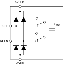
Figure 8-8 illustrates a simplified reference input circuit. Similar to the analog inputs, the reference inputs are protected by ESD diodes. If the reference inputs are driven below AVSS – 0.3 V or above AVDD1 + 0.3 V, the protection diodes can conduct. If these conditions are possible, use external clamp diodes, series resistors, or both to limit the reference input current to the specified value.
 Figure 8-8 Simplified Voltage Reference Input
Circuit
Figure 8-8 Simplified Voltage Reference Input
CircuitThe ADC samples the reference voltage by an internal capacitor (CREF) and then discharges the capacitor at the modulator sampling frequency (fMOD). The sampling operation results in transient current flow into the reference inputs. The transient current is filtered by a 0.1-µF ceramic capacitor placed directly at the reference pins with a larger 10-μF to 47-μF capacitor at the voltage reference output. In applications where the voltage reference drives multiple ADCs, use 0.1-µF capacitors at each ADC.
The external capacitor filters the current transients, resulting in an average reference current. The average reference current is 110 μA/V for high- and mid-power operating modes and 80 μA/V for low-power operating mode. For example, with VREF = 4.096 V, the reference input current is 110 μA / V × 4.096 V = 451 μA.