JAJSH04C May 2013 – March 2019 ADS8866
PRODUCTION DATA.
- 1 特長
- 2 アプリケーション
- 3 概要
- 4 改訂履歴
- 5 概要(続き)
- 6 Device Comparison Table
- 7 Pin Configuration and Functions
- 8 Specifications
- 9 Parameter Measurement Information
- 10Detailed Description
- 11Application and Implementation
- 12Power Supply Recommendations
- 13Layout
- 14デバイスおよびドキュメントのサポート
- 15メカニカル、パッケージ、および注文情報
パッケージ・オプション
メカニカル・データ(パッケージ|ピン)
サーマルパッド・メカニカル・データ
- DRC|10
発注情報
10.4.1.2 4-Wire CS Mode
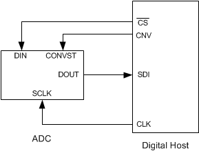
This interface option is useful when one or more ADCs are connected to an SPI-compatible digital host. Figure 45 shows the connection diagram for single ADC; see Figure 47 for the connection diagram for two ADCs.
 Figure 45. Connection Diagram: Single ADC With 4-Wire CS Mode
 In this interface option, DIN is controlled by the digital host and functions as CS. As shown in Figure 46, with DIN high, a CONVST rising edge selects CS mode, forces DOUT to 3-state, samples the input signal, and causes the device to enter a conversion phase. In this interface option, CONVST must be held at a high level from the start of the conversion until all data bits are read. Conversion is done with the internal clock and continues regardless of the state of DIN. As a result, DIN (functioning as CS) can be pulled low to select other devices on the board. However, DIN must be pulled high before the minimum conversion time (tconv-min) elapses and remains high until the maximum possible conversion time (tconv-max) elapses.
 Figure 46. Interface Timing Diagram: Single ADC With 4-Wire CS Mode
 When conversion is complete, the device enters acquisition phase and powers down. DIN (functioning as CS) can be brought low after the maximum conversion time (tconv-max) elapses. On the DIN falling edge, DOUT comes out of 3-state and the device outputs the MSB of the data. The lower data bits are output on subsequent SCLK falling edges. Data can be read at either SCLK falling or rising edges. Note that with any SCLK frequency, reading data at SCLK falling edge requires the digital host to clock in the data during the th_CK_DO-min time frame. DOUT goes to 3-state after the 16th SCLK falling edge or when DIN goes high, whichever occurs first.
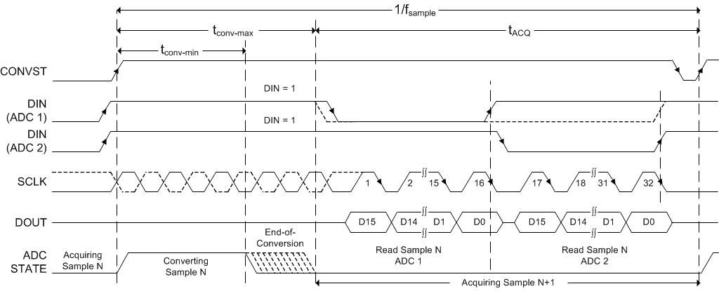
As shown in Figure 47, multiple devices can be hooked together on the same data bus. In this case, as shown in Figure 48, the DIN of the second device (functioning as CS for the second device) can go low after the first device data are read and the DOUT of the first device is in 3-state.
Care must be taken so that CONVST and DIN are not both low together at any time during the cycle.
 Figure 47. Connection Diagram: Two ADCs With 4-Wire CS Mode
  Figure 48. Interface Timing Diagram: Two ADCs With 4-Wire CS Mode