JAJSGQ2F August 2013 – March 2019
PRODUCTION DATA.
- 1 特長
- 2 アプリケーション
- 3 概要
- 4 改訂履歴
- 5 Pin Configuration and Functions
- 6 Specifications
- 7 Detailed Description
- 8 Application and Implementation
- 9 Power Supply Recommendations
- 10Layout
- 11デバイスおよびドキュメントのサポート
- 12メカニカル、パッケージ、および注文情報
パッケージ・オプション
メカニカル・データ(パッケージ|ピン)
- RGR|20
サーマルパッド・メカニカル・データ
- RGR|20
発注情報
7.4.2 Cold-Start Operation (VSTOR < VSTOR_CHGEN, VIN_DC > VIN(CS) and PIN > PIN(CS))
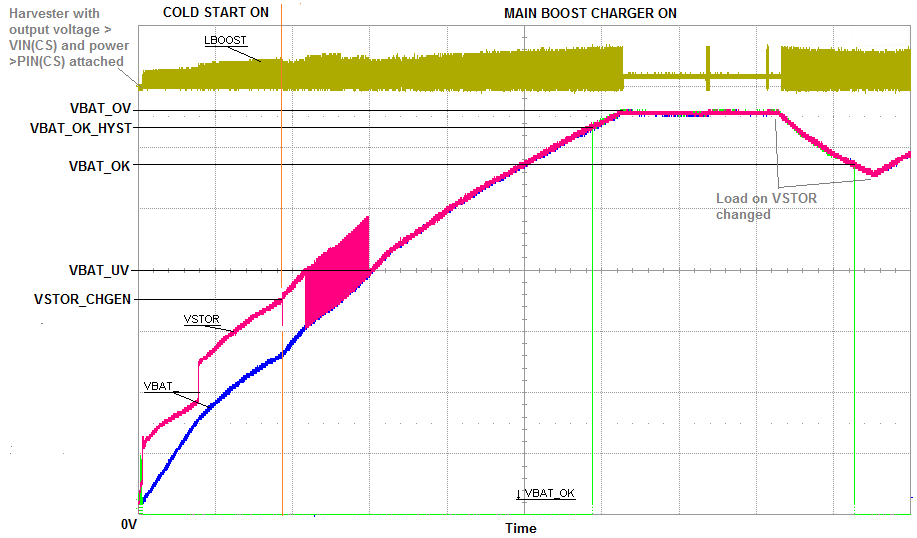
Whenever VSTOR < VSTOR_CHGEN, VIN_DC ≥ VIN(CS) and PIN > PIN(CS), the cold-start circuit is on. This could happen when there is not input power at VIN_DC to prevent the load from discharging the battery or during a large load transient on VSTOR. During cold start, the voltage at VIN_DC is clamped to VIN(CS) so the energy harvester's output current is critical to providing sufficient cold start input power, PIN(CS) = VIN(CS) X IIN(CS). The cold-start circuit is essentially an unregulated, hysteretic boost converter with lower efficiency compared to the main boost charger. None of the other features, including the EN pin, function during cold start operation. The cold start circuit's goal is to charge VSTOR higher than VSTOR_CHGEN so that the main boost charger can operate. When a depleted storage element is initially attached to VBAT_SEC, as shown in Figure 14 and the harvester can provide a voltage > VIN(CS) and total power at least > PIN(CS), assuming no system load or leakage at VSTOR and VBAT_SEC, the cold start circuit can charge VSTOR above VSTOR_CHGEN. Once the VSTOR voltage reaches the VSTOR_CHGEN threshold, the IC
- first performs an initialization pulse on VRDIV to reset the feedback voltages,
- then disables the charger for 32 ms (typical) to allow the VIN_DC voltage to rise to the harvester's open-circuit voltage which will be used as the input voltage regulation reference voltage until the next MPPT sampling cycle and
- lastly performs its first feedback sampling using VRDIV, approximately 64 ms after the initialization pulse.
 Figure 14. Charger Operation After a Depleted Storage Element is Attached and Harvester Power is Available
 The energy harvester must supply sufficient power for the IC to exit cold start. Due to the body diode of the PFET connecting VSTOR and VBAT_SEC, the cold start circuit must charge both the capacitor on CSTOR up to the VSTOR_CHGEN and the storage element connected to VBAT_SEC up to VSTOR_CHGEN less a diode drop. When a rechargeable battery with an open protector is attached, the intial charge time is typically short due to the minimum charge needed to close the battery's protector FETs. When large, discharged super capacitors with high DC leakage currents are attached, the intial charge time can be signficant.
When the VSTOR voltage reaches VSTOR_CHGEN, the main boost charger starts up. When the VSTOR voltage rises to the VBAT_UV threshold, the PMOS switch between VSTOR and VBAT_SEC turns on, which provides additional loading on VSTOR and could result in the VSTOR voltage dropping below both the VBAT_UV threshold and the VSTOR_CHGEN voltage, especially if system loads on VSTOR or VBAT_SEC are active during this time. Therefore, it is not uncommon for the VSTOR voltage waveform to have incremental pulses (for example, stair steps) as the IC cycles between cold-start and main boost charger operation before eventually maintaing VSTOR above VSTOR_CHGEN.
The cold start circuit initially clamps VIN_DC to VIN(CS) = 600 mV typical. If sufficient input power (that is, output current from the harvester clamped to VIN(CS)) is not available, it is possible that the cold start circuit cannot raise the VSTOR voltage above VSTOR_CHGEN in order for the main boost conveter to start up. It is highly recommended to add an external PFET between the system load and VSTOR. An inverted VBAT_OK signal provided by VB_SEC_ON can be used to drive the gate of this system-isolating, external PFET. See the Energy Harvester Selection applications section for guidance on minimum input power requirements.