SNAS811 July 2020 – May CDCE6214
PRODUCTION DATA.
- 1 Features
- 2 Applications
- 3 Description
- 4 Revision History
- 5 Description (cont.)
- 6 Pin Configuration and Functions
-
7 Specifications
- 7.1 Absolute Maximum Ratings
- 7.2 ESD Ratings
- 7.3 Recommended Operating Conditions
- 7.4 Thermal Information
- 7.5 EEPROM Characteristics
- 7.6 Reference Input, Single-Ended Characteristics
- 7.7 Reference Input, Differential Characteristics
- 7.8 Reference Input, Crystal Mode Characteristics
- 7.9 General-Purpose Input Characteristics
- 7.10 Triple Level Input Characteristics
- 7.11 Logic Output Characteristics
- 7.12 Phase Locked Loop Characteristics
- 7.13 Closed-Loop Output Jitter Characteristics
- 7.14 Input and Output Isolation
- 7.15 Buffer Mode Characteristics
- 7.16 PCIe Spread Spectrum Generator
- 7.17 LVCMOS Output Characteristics
- 7.18 LP-HCSL Output Characteristics
- 7.19 LVDS Output Characteristics
- 7.20 Output Synchronization Characteristics
- 7.21 Power-On Reset Characteristics
- 7.22 I2C-Compatible Serial Interface Characteristics
- 7.23 Timing Requirements, I2C-Compatible Serial Interface
- 7.24 Power Supply Characteristics
- 7.25 Typical Characteristics
- 8 Parameter Measurement Information
- 9 Detailed Description
- 10Application and Implementation
- 11Power Supply Recommendations
- 12Layout
- 13Device and Documentation Support
- 14Mechanical, Packaging, and Orderable Information
パッケージ・オプション
メカニカル・データ(パッケージ|ピン)
- RGE|24
サーマルパッド・メカニカル・データ
- RGE|24
発注情報
9.3.3.3 Global and Individual Output Enable
The output enable functionality allows the user to enable or disable all or a specific output buffer. The bypass copy on OUT0 is excluded from the global output enable signal. When an output is disabled, it drives a configurable mute-state. When the serial interface is deactivated one can use all individual output enable signals at the same time. The individual output enable signal controls the respective output channel integer divider to gate the clock, therefore each integer divider must be active.
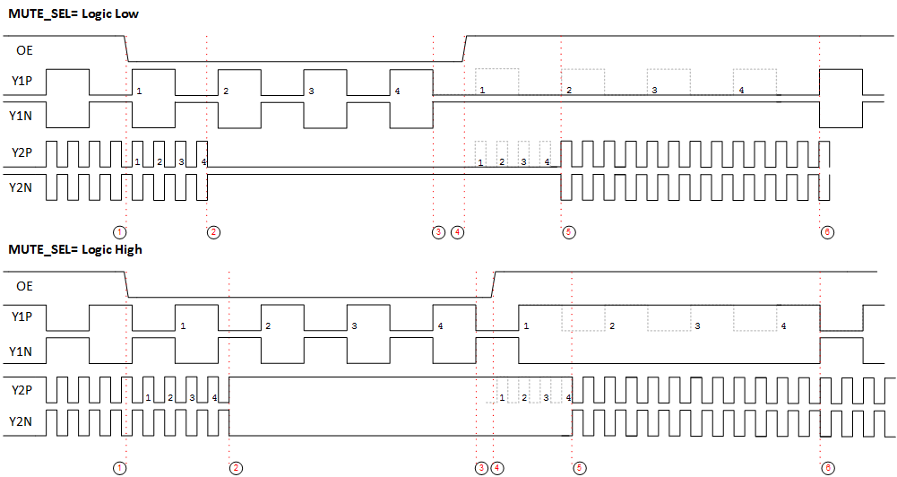
The individual output enable signal enables and disables the respective output in a deterministic way. Therefore the high and low level of the signal is qualified by counting four cycles of the respective output clock.
- The OE falling edge disables the output. The output is enabled for 4 cycles after asserting the Output Enable of a channel. This will enable any further operation in the system after OE is asserted.
- The OE rising edge enables the output. Outputs starts toggling after 4 internal clock cycles.
 Figure 32. Individual Output Enable and Disable
 Table 14. Glitch-less Operation, Divider Synchronization and Global/Individual OE Settings
| REGISTER BIT ADDRESS | REGISTER BIT FIELD NAME | DESCRIPTION |
|---|---|---|
| R0[14] | PDN_INPUT_SEL | Configures PDN pin as PDN or SYNCN |
| R0[5] | SYNC | Generates SYNC signal through serial interface |
| R57[9], R63[9], R68[9], R73[9] | CH1_GLITCHLESS_EN, CH2_GLITCHLESS_EN, CH3_GLITCHLESS_EN, CH4_GLITCHLESS_EN | Enables Glitch-less switching for OUT1/OUT2/OUT3/OUT4 |
| R57[3], R63[3], R68[3], R73[3] | CH1_SYNC_EN, CH2_SYNC_EN, CH3_SYNC_EN, CH4_SYNC_EN | Enables SYNC for OUT1/OUT2/OUT3/OUT4 |
| R57[1], R63[1], R68[1], R73[1] | CH1_MUTESEL, CH2_MUTESEL, CH3_MUTESEL, CH4_MUTESEL | Sets Output level when mute on OUT1/OUT2/OUT3/OUT4 |
| R57[0], R63[0], R68[0], R73[0] | CH1_MUTE, CH2_MUTE, CH3_MUTE, CH4_MUTE | Mutes output on OUT1/OUT2/OUT3/OUT4 |