SNAS811 July 2020 – May CDCE6214
PRODUCTION DATA.
- 1 Features
- 2 Applications
- 3 Description
- 4 Revision History
- 5 Description (cont.)
- 6 Pin Configuration and Functions
-
7 Specifications
- 7.1 Absolute Maximum Ratings
- 7.2 ESD Ratings
- 7.3 Recommended Operating Conditions
- 7.4 Thermal Information
- 7.5 EEPROM Characteristics
- 7.6 Reference Input, Single-Ended Characteristics
- 7.7 Reference Input, Differential Characteristics
- 7.8 Reference Input, Crystal Mode Characteristics
- 7.9 General-Purpose Input Characteristics
- 7.10 Triple Level Input Characteristics
- 7.11 Logic Output Characteristics
- 7.12 Phase Locked Loop Characteristics
- 7.13 Closed-Loop Output Jitter Characteristics
- 7.14 Input and Output Isolation
- 7.15 Buffer Mode Characteristics
- 7.16 PCIe Spread Spectrum Generator
- 7.17 LVCMOS Output Characteristics
- 7.18 LP-HCSL Output Characteristics
- 7.19 LVDS Output Characteristics
- 7.20 Output Synchronization Characteristics
- 7.21 Power-On Reset Characteristics
- 7.22 I2C-Compatible Serial Interface Characteristics
- 7.23 Timing Requirements, I2C-Compatible Serial Interface
- 7.24 Power Supply Characteristics
- 7.25 Typical Characteristics
- 8 Parameter Measurement Information
- 9 Detailed Description
- 10Application and Implementation
- 11Power Supply Recommendations
- 12Layout
- 13Device and Documentation Support
- 14Mechanical, Packaging, and Orderable Information
パッケージ・オプション
メカニカル・データ(パッケージ|ピン)
- RGE|24
サーマルパッド・メカニカル・データ
- RGE|24
発注情報
9.3.1.1 Zero Delay Mode, Internal and External Path
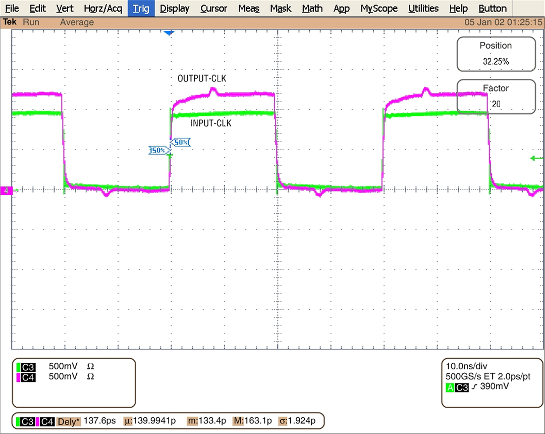
The CDCE6214 can operate in Zero Delay Mode with internal as well as external feedback. In Zero Delay Mode, PRIREF clock is used as the reference clock to the PFD. SECREF input clock can be used to feed an external source as feedback clock to the PFD. External feedback path is recommended for zero delay operation. Moreover there is an additional internal feedback path which is sourced from output channel 2. It is expected that the Input-output propagation delay would be higher in Internal zero-delay mode than external zero delay mode.
Table 2. Zero Delay Operation (1)(2)(3)
| OPERATION | REFSEL | R2[1:0] - REFSEL_SW | R24[1:0] - IP_SECREF_BUF_SEL | R24[15] - IP_PRIREF_BUF_SEL | R0[8] - ZDM_EN | R0[10] - ZDM_CLOCKSEL | DESCRIPTION |
|---|---|---|---|---|---|---|---|
| Normal Operation, XTAL Input | L | 0h or 1h or 2h | 0h | X | 0h | 0h | Normal Operation, XTAL Input |
| Normal Operation, Differential Input | L | 0h or 1h or 2h | 2h or 3h | X | 0h | 0h | SECREF/Differential Input |
| Normal Operation, Differential Input | H | 0h or 1h or 3h | X | 1h | 0h | 0h | PRIREF/Differential Input |
| Normal Operation, LVCMOS Input | L | 0h or 1h or 2h | 1h | X | 0h | 0h | SECREF/LVCMOS Input |
| Normal Operation, LVCMOS Input | H | 0h or 1h or 3h | X | 0h | 0h | 0h | PRIREF/LVCMOS Input |
| External Zero Delay Mode, Differential Input | H | 0h or 1h or 3h | 2h or 3h | 1h | 1h | 1h | Input Clock on PRIREF, Feedback clock on SECREF |
| External Zero Delay Mode, LVCMOS Input | H | 0h or 1h or 3h | 1h | 0h | 1h | 1h | Input Clock on PRIREF, Feedback clock on SECREF |
| Internal Zero Delay Mode, Differential Input | H | 0h or 1h or 3h | X | 1h | 1h | 0h | Input clock on PRIREF |
| Internal Zero Delay Mode, Differential Input | H | 0h or 1h or 3h | X | 0h | 1h | 0h | Input clock in PRIREF |
1. In zero delay mode, all dividers should be programmed such that PLL can lock. On power-up in zero-delay mode, PLL would lock automatically
2. For internal Zero delay mode, channel 2 is required. Channel 2 should not be powered down
3. "X" allows any possible bit-field value. It has no impact on the functionality
 Figure 24. Input/Output Alignment in External Zero Delay Mode for LVCMOS Output